| Posted: Oct 28, 2008 | |
Moth eyes inspire self-cleaning antireflection nanotechnology coatings |
|
| (Nanowerk Spotlight) Antireflection coatings have become one of the key issues for mass production of silicon solar cells. Silicon solar cells are the most common solar cells on the market today. They are constructed with layers of n-type silicon having many electrons and p-type silicon having many electron holes (portions with missing electrons). When hit by sunlight, an equal number of electrons and electron holes are generated at the interface between the two silicon layers and, as the electrons migrate from the n-type silicon to the p-type silicon, an electric flow is generated. | |
| One of the problems with silicon solar cells is the high refractive index of silicon, which causes more than 30% of incident light to be reflected back from the surface of the silicon crystals. Solar cell manufacturers have therefore developed various kinds of antireflection coatings (ARCs) to reduce the unwanted reflective losses. Currently, quarter-wavelength silicon nitride thin films deposited by plasma-enhanced chemical vapor deposition (PECVD) are the industrial standard for ARCs on crystalline silicon substrates. Unfortunately, current top-down lithographic techniques for creating subwavelength silicon gratings, such as electron-beam lithography, nanoimprint lithography, and interference lithography, require sophisticated equipment and are expensive to implement, thus contributing to the still high costs of this type of solar cells. | |
| Borrowing from Mother Nature's millions of years old design book, researchers have now come up with a nanotechnology antireflection coating inspired by the eyes of moths. | |
 |
|
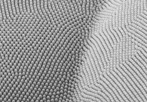
| Details of the moth eye structure. | |
| "We have developed a simple and scalable spin-coating technique that enables wafer-scale production of colloidal crystals with nonclose-packed (ncp) structures" Wei-Lun Min tells Nanowerk. | |
| Min, a student in Peng Jiang's group in the Department of Chemical Engineering at the University of Florida, is first author of a recent paper in Advanced Materials that describes this new coating technique ("Bioinspired Self-Cleaning Antireflection Coatings"). | |
| Min explains that commercial silicon nitride ARCs are typically designed to suppress reflection efficiently at wavelengths around 600 nm. "The reflective loss is rapidly increased for near-infrared and other visible wavelengths, which contain a large portion of the incident solar energy" he says. "In contrast, our subwavelength-structured moth-eye ARCs directly patterned in the substrates are broadband and intrinsically more stable and durable than multilayer ARCs since no foreign material is involved." | |
| The team in Florida has developed a simple and scalable templating technique for making subwavelength ARCs. Knowing that moths use hexagonal arrays of nonclose-packed nipples as antireflection coatings to reduce reflectivity from their compound eyes, they designed a colloidal templating approach for fabricating such moth-eye ARCs on both glass and silicon substrates. | |
| "The outer surface of the corneal lenses of moths consists of ncp arrays of conical protuberances, termed corneal nipples, typically of sub-300nm height and spacing" explains Min. "These arrays of subwavelength nipples generate a graded transition of refractive index, leading to minimized reflection over a broad range of wavelengths and angles of incidence." | |
| In similar fashion, the templated pillar arrays that the researchers designed have a high aspect ratio and exhibit excellent broadband antireflection and nonwetting properties. | |
| The team points out that transparent polymer moth-eye ARCs with good antireflective properties has been demonstrated before but, in contrast to their own ARC, the low aspect ratio (ca. 0.5) of the previously templated nipples had hampered the realization of superhydrophobic coatings. | |
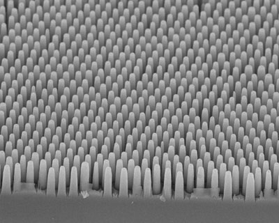
| In their approach, Min and his colleagues used a simple and scalable spin-coating technique to generate ncp colloidal monolayers of hexagonally ordered silica particles on silicon wafers. These particles are then used as etching mask during a reactive ion etch (RIE). | |
 |
|
| Templated silicon pillar arrays. (Image: Wei-Lun Min, University of Florida) | |
| "As the etching rate of silica is much lower than that of silicon under RIE conditions, silica particles protect silicon immediately underneath them from being etched, resulting in the formation of pillar arrays directly on silicon surface" Min explains the process. | |
| Once the silicon pillars are deep enough, the process is stopped by removing the templating silica spheres with a solution. | |
| Min points out that their technique can be easily utilized to generate wafer-scale silicon pillar arrays, is compatible with standard industrial manufacturing and is promising for developing self-cleaning ARCs for a large variety of technological applications ranging from solar cells and photodiodes to flat panel displays and optical components. | |
 By
Michael
Berger
– Michael is author of three books by the Royal Society of Chemistry:
Nano-Society: Pushing the Boundaries of Technology,
Nanotechnology: The Future is Tiny, and
Nanoengineering: The Skills and Tools Making Technology Invisible
Copyright ©
Nanowerk LLC
By
Michael
Berger
– Michael is author of three books by the Royal Society of Chemistry:
Nano-Society: Pushing the Boundaries of Technology,
Nanotechnology: The Future is Tiny, and
Nanoengineering: The Skills and Tools Making Technology Invisible
Copyright ©
Nanowerk LLC
|
Become a Spotlight guest author! Join our large and growing group of guest contributors. Have you just published a scientific paper or have other exciting developments to share with the nanotechnology community? Here is how to publish on nanowerk.com.