| Posted: Dec 11, 2013 |
Flexible thermoelectric generator from bulk silicon |
| (Nanowerk Spotlight) Today’s digital world is dominated mainly by silicon-based electronics. Silicon offers a unique combination between mechanical and electrical properties making it one of the most developed materials in semiconductor industry. However, silicon is brittle and cannot be flexed, hindering its potential for high performance electronics that is flexible, stretchable or applied to irregular shapes. |
| Researchers at the King Abdullah University of Science and Technology (KAUST) in Saudi Arabia have now developed a pragmatic approach to achieve high performance integrated electronic systems, including thermoelectric energy harvesters, onto flexible silicon substrates. |
| "With our approach, we can build devices using well-established silicon technology to avoid compromising performance and then transfer them using simple micro-fabrication processes which enables batch processing of peeled off flexible silicon of various thicknesses," Muhammad Mustafa Hussain, an Associate Professor of Electrical Engineering at KAUST, tells Nanowerk. "These processes are not expensive, do not require expensive substrates and do not damage the devices. Additionally, the unused bulk bottom portion of the silicon wafer is available for further use." |
| Although the process, reported in a recent edition of Small ("Flexible and Semi-Transparent Thermoelectric Energy Harvesters from Low Cost Bulk Silicon (100)") seems simple and common, it is novel and uniquely used for the first time for the demonstrated purposes. |
| "We foresee more exciting applications in flexible electronics rooted from this generic process," says Galo Torres Sevilla, a PhD student in Hussain's group and the paper's first author. "Being able to transform silicon onto a flexible platform allows to integrate all types of electronic components." |
| In this work, the KAUST team demonstrates the integration of thermoelectric generators onto a flexible silicon platform using only state-of-the-art and industry compatible fabrication processes. |
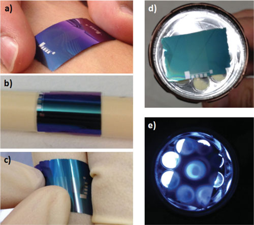 |
| Flexibility and transparency from peeled silicon integrated with thermoelectric energy harvesters. a) Image of a peeled-off 2 cm × 1.5 cm mono-crystalline silicon (100) piece of 18 µm thickness with 63 integrated thermoelectric couples for energy harvesting on a wrist skin. b) Extreme bending and stiction of the same piece around a plastic ball pen due to the van der Walls force. c) In addition to bending we also show the durability of the sample by wrapping the same piece on a finger–proving its effectiveness for wearable medical electronics. Presence of various films like silicon oxide, aluminum oxide, bismuth telluride, antimony telluride, titanium and aluminum are not contributing significantly to exert enough stress to deform the peeled silicon piece. d) One of the interesting aspects of the peeled silicon is it is not rolling over when it is placed freely on the smoothly flat surface of a LED based torch. e) When the torch is ON, the lights are visible through the peeled silicon integrated with device showing its semi-transparent nature due to the hole creation to perform the peel off operation. (Reprinted with permission from Wiley-VCH Verlag) |
| Flexible thermoelectric generators (TEGs) have virtually unlimited number of applications in consumer electronics. However, in order to make use of all the advantages that they offer in terms of flexibility and increased power generation, they may be used in applications where systems need to be integrated in hostile and difficult to access locations. Specifically, they may be used in implantable electronics, wearable electronics, or remote sensing systems. Their complete solid-state characteristic makes them devices that need extremely low maintenance and hence a cheap and pragmatic way to obtain energy out of waste heat. |
| "We believe that the demonstration of flexible thermoelectric generators on silicon gives a step forward towards monolithic integration of flexible systems-on-chip, specially for applications where access is difficult and where batteries are just a temporary, expensive and complicated solution," notes Hussain. |
| The lateral TEG was fabricated first on low-cost bulk mono-crystalline silicon (100) followed by transforming the TEG and the hosting silicon into a flexible and transparent system using a state-of-the-art CMOS compatible process. The released flexible and transparent silicon fabric is 18 mm thick with 63 thermopiles. |
| The remaining wafer was then reused after appropriate chemical mechanical polishing (CMP). The TEGs on released flexible and transparent silicon fabric shows 30 times more power (0.15 mW) generation than TEGs located on a solid silicon substrate. |
| "The main difference with previous demonstrations using SOI or Si (111) wafers is we can transfer the whole flexible silicon circuitry after the conventional fabrication of complicated multi-level interconnects is completed," explains Torres Sevilla. "Although two groups have recently demonstrated mechanical exfoliation of silicon chips, in all cases doping diffusion – highly expensive high energy implantation – was used prior to any device fabrication and by nature the devices are opaque." |
| According to the team, the power generated by these thermoelectric energy harvesters is sufficient to run ultra-low power CMOS circuitry for sensors and possible in-vivo bio-medical electronics. |
| "Going forward, we would like to integrate a complete system that can power itself and at the same time compete with today’s high performance electronics by taking advantage of our silicon based integration process," Hussain describes the team's goal for the future. "The main challenge will be to integrate the different modules into a single chip with the highest yield possible. However, we are confident that we soon will be able to demonstrate a flexible standalone system that makes use of the most advanced semiconductor material, silicon, for complete monolithic integration." |
 By
Michael
Berger
– Michael is author of four books by the Royal Society of Chemistry:
Nano-Society: Pushing the Boundaries of Technology (2009),
Nanotechnology: The Future is Tiny (2016),
Nanoengineering: The Skills and Tools Making Technology Invisible (2019), and
Waste not! How Nanotechnologies Can Increase Efficiencies Throughout Society (2025)
Copyright ©
Nanowerk LLC
By
Michael
Berger
– Michael is author of four books by the Royal Society of Chemistry:
Nano-Society: Pushing the Boundaries of Technology (2009),
Nanotechnology: The Future is Tiny (2016),
Nanoengineering: The Skills and Tools Making Technology Invisible (2019), and
Waste not! How Nanotechnologies Can Increase Efficiencies Throughout Society (2025)
Copyright ©
Nanowerk LLC
|

Become a Spotlight guest author! Join our large and growing group of guest contributors. Have you just published a scientific paper or have other exciting developments to share with the nanotechnology community? Here is how to publish on nanowerk.com. |
