| Posted: Feb 02, 2018 |
Kirigami nanofluidic devices |
| (Nanowerk Spotlight) Recent research in nanofluidics has adopted reconstructed layered two-dimensional (2D) sheets (such as graphene oxide or clay) as a promising material platform. These membranes contain a high volume fraction of interconnected 2D nanochannels. Fabricating these nanochannels is straightforward and scalable, and does not rely on lithography or etching. |
| "Compared to other scalable nanofluidic materials such as anodized aluminum oxide membrane, block copolymer membrane and nanofluidic crystals, a unique feature of such layered membranes is that the channels are horizontally aligned and the channel height (i.e., interlayer spacing), which is responsible for confinement of the electrolyte, remains uniform throughout the entire thin-film," Jiaxing Huang, a Professor of Materials Science and Engineering at Northwestern University, tells Nanowerk. "Therefore, nanofluidic ionic transport properties are maintained regardless of the lateral dimensions or shape of the 2D nanochannel network." |
| The researchers termed this process, which opens up a range of new opportunities for manipulating ionic transport by tailoring the shape of the films, kirigami nanofluidics. They reported their findings in Materials Chemistry Frontiers ("Kirigami nanofluidics"). |
| The work shows that these 2D membranes behave like 'ionic wafers', which can be patterned by kirigami to realize device functions such as diodes. |
| "Although these ionic functions are still quite simple, compared to electronic devices, they show that ionic transport through a layered membrane, which is a nanoscale phenomenon, could be tuned by tailor cutting the macroscopic shape of the film," notes Jun Gao, the paper's first author. "We hope that the mechanistic understanding and the demonstrations in this work can help people better understand ionic transport through these 2D films, which is useful for designing large scale nanofluidic channels arrays for separation purposes." |
| Compared to the classical ionic diodes, which typically are made of channels with asymmetric ends such as conical nanopores (Figure 1a), the 2D nanochannels have uniform channel size throughout the entire volume of the film. This simplifies the factors affecting ionic transport, making it possible to control the overall ionic conductance by tailoring the ionic resistance at the channel-reservoir interface. |
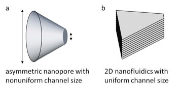 |
| Figure 1: Schematic drawings highlighting the microstructural differences between (a) a conical-shaped nanopore, whose channel size is nonuniform and (b) a GO film that has uniform channel size, despite of asymmetric macroscopic shape. (© RSC) |
| For example, a graphene oxide film with asymmetric ends, such as a T-shape, exhibits ionic rectification (Figure 2d). Whereas shapes with symmetric ends, such as a diode-sign, exhibit no rectification (Figure 2c). |
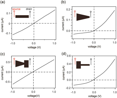 |
| Figure 2: Kirigami nanofluidic devices. (a) A rectangular piece of GO paper shows symmetric current under both forward and reverse bias. (b) When cut into a trapezoidal shape, the device rectifies the current, exhibiting typical diode-like behavior. (c) A piece of GO paper with the shape of a 'diode sign' does not show rectifying behavior. (d) A T-shaped GO paper shows a diode-like rectifying current. The insets illustrate the top view of the GO papers. For consistency, the left reservoirs of all devices are designated as the source. These results suggest that current rectification is only determined by the relative widths of the two ends, and not by the shape of the GO paper in between. (© RSC) |
| Kirigami nanofluidics allows the fabrication of nanofluidic devices and the control of their performance in a very straightforward way. For example, the ionic current rectification ratio can be adjusted by 'tailor cutting' the geometry of the film, which has been quite difficult in previous works. |
| Nanofluidic devices are ionic analogs to semiconductor devices. Kirigami-made resistors and diodes can be connected to realize some simple logic functions like the AND gate and OR gate. |
| "An electrolyte confined in nanochannels exhibits unusual behaviors owing to strong influences from the channel walls," explains Erik Luijten, a Professor of Materials Science and Engineering at Northwestern University. "When the size of a charged channel is comparable to the Debye length of the electrolyte, co-ions are effectively repelled from the channel and counterions are concentrated, leading to the so called unipolar ionic transport properties with the counterions as the majority charge carrier." |
| The team first hypothesized that such nanochannels can be readily formed by stacking up 2D sheets, such as graphene oxide. Indeed, they had previously demonstrated that films of graphene oxide or clay sheets contain massive arrays of parallel 2D nanofluidic channels. |
| In this regard, films of 2D sheets are conceptually analogous to extrinsically doped semiconductors, a material foundation that has enabled the realization of numerous electronic devices and integrated circuits. |
| In the current work, Huang's team showed that, like semiconductor wafers, films of graphene oxide can also be 'patterned' to realize some analogous functions such as ionic diodes or logic circuits. The patterning is done by cutting the film into various shapes. |
| In one demonstration, Huang's team showed that programmable rectification ratio can be realized in multi-armed films, by varying the numbers of arms for the source and drain, respectively. |
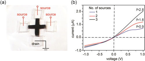 |
| Figure 3. Programming the rectification ratio. (a) Photo showing a cross-shaped GO paper with four branches. One branch is designated as the drain. By varying the number of branches that are connected to the source, the rectification ratio f can be tuned. (b) Current?voltage measurements show that the forward current varies in direct proportion to the number of source branches used. The reverse-voltage resistance is determined mostly by the edge length of the drain end and therefore remains largely unchanged (© RSC) |
| Going forward, the scientists are interested in creating nanofluidic devices with active gating function, which would allow them to manipulate nanofluidic transport with more freedom. |
| Monica Olvera de la Cruz, a co-author of the paper and a Professor of Materials Science and Engineering at Northwestern University, concludes that "It will be very exciting to realize some form of gating mechanism to make ionic transistors, and to integrate all of these device elements to achieve more complex logic or even computing functions." |
 By
Michael
Berger
– Michael is author of four books by the Royal Society of Chemistry:
Nano-Society: Pushing the Boundaries of Technology (2009),
Nanotechnology: The Future is Tiny (2016),
Nanoengineering: The Skills and Tools Making Technology Invisible (2019), and
Waste not! How Nanotechnologies Can Increase Efficiencies Throughout Society (2025)
Copyright ©
Nanowerk LLC
By
Michael
Berger
– Michael is author of four books by the Royal Society of Chemistry:
Nano-Society: Pushing the Boundaries of Technology (2009),
Nanotechnology: The Future is Tiny (2016),
Nanoengineering: The Skills and Tools Making Technology Invisible (2019), and
Waste not! How Nanotechnologies Can Increase Efficiencies Throughout Society (2025)
Copyright ©
Nanowerk LLC
|

Become a Spotlight guest author! Join our large and growing group of guest contributors. Have you just published a scientific paper or have other exciting developments to share with the nanotechnology community? Here is how to publish on nanowerk.com. |
