| Posted: Jun 22, 2011 | |
Laser-based nanoparticle processing for nanoelectronics fabrication |
|
| (Nanowerk Spotlight) Many applications in the electronics industry require some form of micro- or nanopatterning technique in fabricating the devices, structures and surfaces required. And although they may not be visible to the naked eye, the micro- and nanometer-sized trenches, ridges, curves and grooves of these patterns and surfaces have a very visible impact on the functionality of the device. | |
| Conventional metal patterning in the electronics industry is done by a photo-resist patterning with a photo-mask and metal evaporation in a vacuum chamber (photolithography). This technology require expensive vacuum conditions, high processing temperatures, many steps, and toxic chemicals to fabricate one layer of a metal pattern. Furthermore, it is almost impossible to change the design of the expensive photomask once it is fabricated. | |
| Researchers have now developed a high-resolution metal nano-patterning technique by combining solution deposited metal nanoparticles and a femtosecond laser without using conventional vacuum deposition or photo-masks. With this method, the time and cost associated with high-resolution metal patterning can be reduced dramatically without using time-consuming vacuum processes and the pattern design can be easily changed in a digital manner without using expensive photo-masks. | |
| Back in 2007, we reported on a metal direct patterning techniques by a continuous laser sintering of the same metal nanoparticles used in this new research (see "An ultralow-cost, large area way for nanoelectronics fabrication"). Back then, though, the resolution of the metal patterns was limited to several microns at most due to large heat diffusion and light diffraction limit. | |
| The team has now improved their technique and demonstrated nanoscale feature fabrication with a ultra-short pulsed laser. | |
| "As a potential alternative to e-beam lithography, we have introduced a novel digital, low-temperature, high-resolution, direct metal patterning method wherein solution-deposited metal nanoparticles are sintered by applying a femtosecond laser for the fabrication of nanoscale electronics," Seung Hwan Ko, a professor in the Department of Mechanical and Aerospace Engineering at Korea Advanced Institute of Science and Technology (KAIST), explains to Nanowerk. "For the first time, we demonstrate high-resolution nanoscale metal patterns made using a femtosecond laser from solution-deposited metal nanoparticles, overcoming the light diffraction limit." | |
| As the team reports in a recent issue of Advanced Materials ("Nanoscale Electronics: Digital Fabrication by Direct Femtosecond Laser Processing of Metal Nanoparticles"), this significant advance in resolution could be achieved due to the combination of the short pulse nature of the femtosecond laser and the novel thermal characteristics of the metal nanoparticles. | |
 |
|
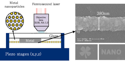
| Process schematics of the femtosecond laser selective nanoparticle sintering (left figure) and the SEM pictures of the fabricated nanoscale metal feastures (right figures). (Image: Dr. Seung Hwan Ko, KAIST) | |
| "Our approach offers the remarkable advantages of a one-step, direct, high-resolution process that may be applicable to nanoscale electronics" says Ko. "The main motivation of our current work was to reduce the heat affected zone by ultra short pulsed laser therefore to reduce the metal patterning size. Ultra short pulsed laser such as a femtosecond laser can minimize the thermal effect because the laser pulse duration (10-15 second) is much shorter than the material heating time (>10-12 second) and therefore the nanoparticle heating by laser was finished before the material feel the heat." | |
| Ko describes the direct femtosecond laser selective nanoparticle sintering (FLSNS) process, as illustrated in above figure: "We spin-coated silver nanoparticle ink onto a cover glass or a silicon wafer substrate to form a nanoparticle thin-film. This thin-film was selectively melted by scanning the focused femtosecond laser beam. Upon completion of the FLSNS process, the remaining unmelted and not laser-processed silver nanoparticles were simply washed away in the organic solvent to leave laser processed metal nano- and micropatterns." | |
| Ko notes that the shape and resolution of the metal patterns fabricated by the FLSNS process are dependent on various fabrication conditions, including the position of the laser beam focus, the laser beam intensity, and the scanning speed. | |
| He points out that the significant advance in resolution enhancement by the FLSNS process over metal nanoparticle inkjet printing or selective continuous wave laser sintering processes could be achieved mainly due to the combination of the ultrashort pulse nature of femtosecond laser and the novel thermal characteristics of the metal nanoparticles. | |
| Although the size of the patterned area was limited to several hundreds of microns due to the travel distance limitation of the piezo-electrically driven stage, the researchers say that the patterning area can be further expanded by combining a macroscale translation stage and a nanoscale scale stage. | |
| This FLSNS technique can make nanoscale metal patterning via a single, simple process and can potentially be used as a lower-cost alternative to very expensive electron beam lithography systems. | |
| "Our approach may achieve the same high resolution as electron lithography at a much faster speed – more than 10 times – and in a more versatile non-vacuum environment," says Ko. "Furthermore, the process temperature is lower than 150°C and this process can be applied to the metal patterning on heat sensitive materials such as plastic substrates or biomaterials." | |
| In their current work, the team has demonstrated 2D metal patterning. They are now trying to expand this current technique to 3D metal structuring. | |
| "However, 3D metal structuring is not easy because the interaction of the metal nanoparticle with laser is very strong and there is a high probability for the preprocessed underlying layer to be damaged by the following processing laser," says Ko. | |
 By
Michael
Berger
– Michael is author of three books by the Royal Society of Chemistry:
Nano-Society: Pushing the Boundaries of Technology,
Nanotechnology: The Future is Tiny, and
Nanoengineering: The Skills and Tools Making Technology Invisible
Copyright ©
Nanowerk LLC
By
Michael
Berger
– Michael is author of three books by the Royal Society of Chemistry:
Nano-Society: Pushing the Boundaries of Technology,
Nanotechnology: The Future is Tiny, and
Nanoengineering: The Skills and Tools Making Technology Invisible
Copyright ©
Nanowerk LLC
|
|
|
Become a Spotlight guest author! Join our large and growing group of guest contributors. Have you just published a scientific paper or have other exciting developments to share with the nanotechnology community? Here is how to publish on nanowerk.com. |
|