| Posted: Aug 22, 2013 | |
Nanotechnology research produces foldable graphene electronics on paper |
|
| (Nanowerk Spotlight) In contrast to flexible electronics, which rely on bendable substrates, truly foldable electronics require a foldable substrate with a very stable conductor that can withstand folding, i.e. an edge in the substrate at the point of the fold, which develops creases, and the deformation remains even after unfolding. That means that, in addition to a foldable substrate like paper, the conductor that is deposited on this substrate also needs to be foldable. | |
| Paper, the ultimate foldable substrate, has already been explored to replace plastic substrates as a lightweight substrate for low-cost, versatile, and roll-to-roll printed electronics (read more: "Nanopaper transistors for the coming age of flexible and transparent electronics"). For instance, nanotechnology researchers have already printed solar cells on paper ("Mass-printed polymer/fullerene solar cells on paper") and built paper batteries ("Truly green paper battery is algae-powered"). | |
| In a recent paper in Advanced Materials ("Foldable Graphene Electronic Circuits Based on Paper Substrates"), researchers have now demonstrated a fabrication process for foldable graphene circuits based on paper substrates. | |
| While some groups have demonstrated ink-jet printed graphene circuits on paper by using a graphene dispersion (see for instance: "Inkjet printing of graphene for flexible electronics"), the ability to control the thickness of the deposited graphene with this method has proven to be quite difficult. The new technique, developed by a research team from Korea Advanced Institute of Science and Dankook University, led by Byung Doo Chin, has employed a transfer printing process to prevent direct contact of the solvent and paper and to easily control the thickness of the deposited graphene. | |
 |
|
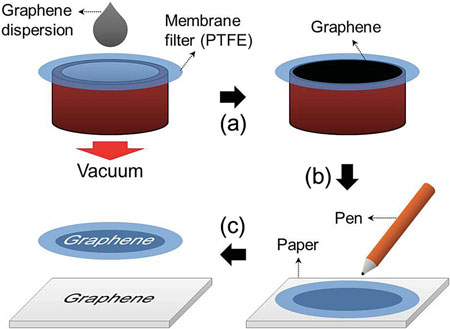
| Steps in the preparation of a graphene circuit on a paper substrate via vacuum filtration of a dispersion of graphene nanoplates and a selective transfer process with a pen. a) The graphene dispersion was filtered by a PTFE membrane filter. b) After turning the filter over and placing it on paper, circuits were drawn on the back of the membrane filter by a pen. c) The membrane filter was removed from the paper substrate. (Reprinted with permission from Wiley-VCH Verlag) | |
| "The fabrication process for graphene circuits contains several advantages including easy control of the circuit width, no need for a specialized mask for complexly patterned circuits, and simple modification" write the authors. "Furthermore, the thickness of the circuits can be adjusted just by varying the amount of the graphene dispersion introduced for vacuum filtration. The thickness was directly proportional to the graphene dispersion and the sheet resistance was decreased with increasing thickness. In this way, we can easily control the dimensions of the graphene circuits." | |
| Experimenting with various dispersions and surfactants, the team tested the factors that affect the adhesion between the transferred graphene and the paper. They defined three works of adhesion and cohesion in the selective transfer process can be defined, which are works of adhesion between the membrane filter and the graphene (WFG), adhesion between the paper substrate and the graphene (WPG), and cohesion between the graphene nanoplates (WGG). | |
| "For successful transfer printing, WFG should be less than WPG), which could be accomplished by the introduction of PSS (poly(4-styrenesulfonic acid)) on the surface of the graphene nanoplates," the researchers explain their findings. "Moreover, the result, that graphene was transferred from the membrane filter onto the paper substrate only in the area where the shapes of the circuits were drawn on the back of the filter, implies that WGG is less than both WFG and WPG)." | |
| They explain that their fabrication process for graphene circuits contains several advantages: easy control of the circuit width; no need for a specialized mask for complexly patterned circuits; simple modification; and that the thickness of the circuits can be adjusted just by varying the amount of the graphene dispersion introduced for vacuum filtration. | |
| "The thickness was directly proportional to the graphene dispersion and the sheet resistance was decreased with increasing thickness," they note. "In this way, we can easily control the dimensions of the graphene circuits." | |
 |
|
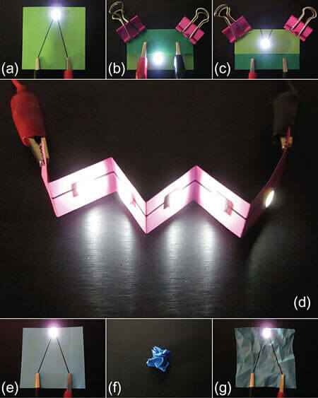
| Photographs of applications. a,b,c) Operation of a LED chip with graphene circuits on a paper substrate under -180° folding and 180° folding. d) Array of LED chips on a three-dimensional circuit board including negative and positive angle folding. e,f,g) Operation of a LED chip on the paper-based circuit board before and after crumpling. (Reprinted with permission from Wiley-VCH Verlag) | |
| The electronic circuits revealed a small change in conductance under various folding angles and maintained an electronic path on the paper substrate after repetitive folding and unfolding. | |
| Employing the graphene circuits, the team demonstrated foldable circuit boards based on paper substrates for operating LED chips under various kinds of deformation. | |
| "We believe that our approach could provide a meaningful method for a simple patterning of the dispersion-based graphene conductor to realize highly potential applications based on paper substrates," they conclude their findings. | |
 By
Michael
Berger
– Michael is author of three books by the Royal Society of Chemistry:
Nano-Society: Pushing the Boundaries of Technology,
Nanotechnology: The Future is Tiny, and
Nanoengineering: The Skills and Tools Making Technology Invisible
Copyright ©
Nanowerk LLC
By
Michael
Berger
– Michael is author of three books by the Royal Society of Chemistry:
Nano-Society: Pushing the Boundaries of Technology,
Nanotechnology: The Future is Tiny, and
Nanoengineering: The Skills and Tools Making Technology Invisible
Copyright ©
Nanowerk LLC
|
|
|
Become a Spotlight guest author! Join our large and growing group of guest contributors. Have you just published a scientific paper or have other exciting developments to share with the nanotechnology community? Here is how to publish on nanowerk.com. |
|