| Posted: Jan 23, 2015 | |
Fully transparent, rollable electronics built with a graphene/carbon nanotube backbone |
|
| (Nanowerk Spotlight) The coming age of wearable, highly flexible and transparent electronic devices will rely on essentially invisible electronic and optoelectronic circuits. In order to have close to invisible circuitry, one must have optically transparent thin-film transistors (TFTs). In order to have flexibility, one needs bendable substrates. | |
| Both flexible electronics and transparent electronics have been demonstrated before, but never rollable electronics that are also fully transparent at the same time. | |
| This has now been achieved by a team of researchers in Korea, who have successfully built rollable and transparent electronic devices that are not only lightweight, but also don't break easily. | |
| To manufacture flexible electronics, one needs a starting material – the substrate – on which to build-up the device. In order for the final product to be flexible, the substrate of course also has to be flexible. In fact, it is the substrate that determines, to a large extent, the overall flexibility of the final product. | |
| So if the substrate is flexible to an extent of being rollable – which can be achieved making it very thin – the final product will also, to some extent, be rollable. Of course, the semiconductors, dielectrics, and metals making up the electronic device, should also be similarly flexible (or soft), otherwise faults will occur. | |
| Plastics are the obvious choice for flexible substrates as the substrates are also required to be insulating (nonconductive) in most applications. Other obvious advantages of plastics are that they are lightweight and non-breakable. | |
| A team led by Professor Jin Jang, Director of the Department of Information Display at Kyung Hee University, has achieved this by overcoming two major challenges associated with the manufacture of flexible electronics: The temperature restriction of plastic substrates (<100°C) and the difficulty of handling flexible electronics during the fabrication process. They reported their findings in ACS Applied Materials & Interfaces ("Fully Transparent and Rollable Electronics"). | |
 |
|
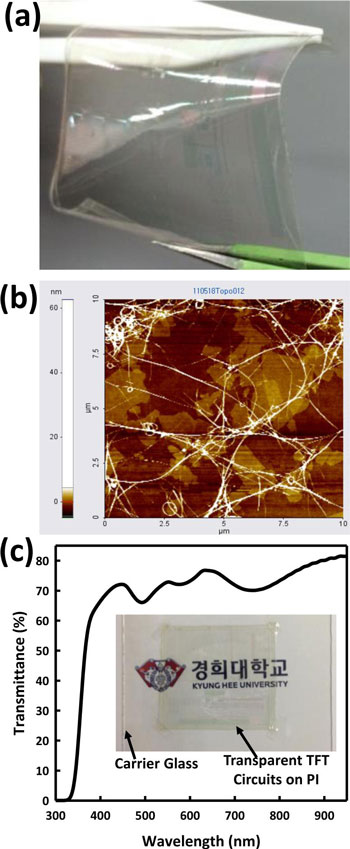
| Fully transparent and rollable circuits: (a) Image of fabricated fully transparent and rollable a-IGZO TFT circuits after detachment from carrier glass; (b) atomic force microscope image obtained from the backside of the CPI substrate with the CNT/GO backbone; (c) optical transmittance of the a-IGZO TFT circuits. Inset shows transparency of the rollable a-IGZO TFT devices attached to a carrier glass. (Reprinted with permission by American Chemical Society) | |
| "To overcome the temperature restriction we chose our plastic substrate to be polyimide (PI), which is a polymer of imide monomers," Jang explains to Nanowerk. "PI has high chemical and heat resistance and when it is colorless, which is the case of this research, it withstands processing temperatures around 300°C." | |
| The researchers also chose an amorphous oxide semiconductor – amorphous-indium-gallium-zinc-oxide (a-IGZO) – which assures good device performance even when sputter-deposited at low temperatures. | |
| For consistency, they also chose a zinc-based metal, indium-zinc-oxide (IZO), for the metal electrodes – i.e. the gate, source, and drain electrodes of the field-effect transistors making up the electronic devices. | |
| "Both the a-IGZO and IZO have large band-gaps, and therefore, are transparent to visible light," says Jang. "As the dielectrics are also transparent and the substrate (PI) is colorless, the final product is see-through with a transmittance of 70% for the full circuit device. The colorless PI (CPI) is 15 µm thick and the thickness of the electronic devices is ∼1 µm, resulting in a total thickness of the fabricated thin-film transistor of only ∼16 µm. Hence, the electronic devices are rollable." | |
| In order to deal with the second major challenge – the difficulty of handling flexible electronics during the fabrication process – the researchers used a carrier glass substrate on which the CPI is first spin-coated from solution, and then detached from after device fabrication. | |
| Being around 0.7 mm in thickness, the carrier glass is rigid enough to provide mechanical support for the CPI, without which accurate layer registration is impossible during photolithography. This is because standalone plastics substrates can warp, shrink, or bulge at high temperatures. | |
| "A rigid carrier substrate is, therefore, a necessity when vacuum processes and photolithography are involved," Jang notes. "However, the way the flexible substrate is attached to the rigid carrier substrate is important as it has to be detached from the carrier substrate after device fabrication. The use of adhesive materials/glues to attach flexible substrates to carrier substrates is not recommended as most adhesives cannot withstand high processing temperatures." | |
| An alternative method is to spin-coat the flexible substrate from solution onto the carrier substrate. Although this method avoids the use of adhesive materials, it is very difficult to detach the flexible substrate from the carrier substrate afterwards because bonds between the two have a tendency of strengthening during the fabrication process. | |
| "The current solution is to deposit a thin layer such as amorphous-silicon between the flexible substrate and the carrier substrate, which can be evaporated by a laser to release the flexible substrate from the carrier substrate after device fabrication," says Jang. "Given the high cost of installing laser equipment, the complexity of the laser detachment process, and the limitations of the laser beam size, we felt their was a need for a better method." | |
| In their research, Jang's team do not use adhesive material or lasers. Neither do they deposit a layer of amorphous-silicon between the carrier glass and the CPI. Instead, they spin coat a mixture of carbon nanotubes and graphene oxide (GO) to a thickness of 1 nm from solution onto of the carrier glass before spin coating the CPI. | |
| "As the CNT/GO layer has a flake like structure with CNT links, it decreases the area where the CPI contacts the glass, thereby reducing its adhesion to glass," explains Jang. "Inserting the CNT/GO layer also doesn't cost much because only a few drops are required to achieve a thickness around 1 nm." | |
| After fabrication, only a small amount of mechanical force is required to detach the CPI from the glass. According to the scientists, the beauty of having the CNT/GO layer is that it bonds stronger with the CPI compared to the glass, such that it remains embedded to the backside of the CPI after detachment – providing mechanical support to the flexible electronics and making the rollable electronics wrinkle-free. | |
| Electronic devices built on plastic substrates are prone to electrostatic discharge (ESD) damage because plastics are usually associated with the generation of electrostatic charge. By contrast, the CPI in this present work is ESD-free because localized ESD can be released via the conductive CNT. | |
| In their experiments, the team rolled the TFT devices 100 times on a cylinder with radius of 4 mm, without significantly degrading their performance. Integrated circuits also operated without degradation, while being bent to a radius of 2 mm, making these devices suitable for transparent and rollable displays. | |
 By
Michael
Berger
– Michael is author of three books by the Royal Society of Chemistry:
Nano-Society: Pushing the Boundaries of Technology,
Nanotechnology: The Future is Tiny, and
Nanoengineering: The Skills and Tools Making Technology Invisible
Copyright ©
Nanowerk LLC
By
Michael
Berger
– Michael is author of three books by the Royal Society of Chemistry:
Nano-Society: Pushing the Boundaries of Technology,
Nanotechnology: The Future is Tiny, and
Nanoengineering: The Skills and Tools Making Technology Invisible
Copyright ©
Nanowerk LLC
|
|
|
Become a Spotlight guest author! Join our large and growing group of guest contributors. Have you just published a scientific paper or have other exciting developments to share with the nanotechnology community? Here is how to publish on nanowerk.com. |
|