| Posted: Dec 30, 2008 | |
Just looking at graphene can change its properties |
|
| (Nanowerk Spotlight) Graphene is a recently discovered allotrope of carbon, which consists of a planar single sheet of carbon atoms arranged in honeycomb lattice. It has attracted tremendous attention of the nanotechnology research community owing to a number of unique physical properties. From a practical point of view, some of the most interesting characteristics of graphene are its extraordinarily high room temperature carrier mobility and recently measured extremely high thermal conductivity (see 'Cool' graphene might be ideal for thermal management in nanoelectronics). | |
| The outstanding current and heat conduction properties of graphene are beneficial for the proposed electronic, interconnect, and thermal management applications. There is a realistic possibility that soon the fastest transistors and most sensitive detectors will be made out of graphene. For instance, we have just reported that next generation computer memory could be made of graphene. | |
| In order to build useful devices from materials which have only atomic thickness (as small as 0.35 nanometers) – as single-layer graphene does – one has to use extensively scanning electron microscopy (SEM), transmission electron microscopy (TEM) and focused ion beam (FIB) processing. Unfortunately, all material characterization techniques which involve electron beam irradiation of the samples may result in damage to the material and disordering of the crystalline lattice. So far, despite the practical importance of the issue, the scale of this potential damage to single-layer or bi-layer graphene has not been investigated. What happens with the crystalline lattice has also been unclear. | |
| Alexander A. Balandin, Professor of Electrical Engineering at the University of California, Riverside (UCR), together with his graduate student Desalegne Teweldebrhan, has discovered that even short-time (a few minutes) exposure of graphene to low and medium energy electron-beam irradiation (5 - 20 keV), which is typical of SEM characterization, results in substantial changes of graphene's properties. Even small doses of irradiation strongly deteriorate graphene's ability to conduct electric current. In this sense, just looking at graphene can change its properties. But you would need an electron microscope for that. | |
 |
|
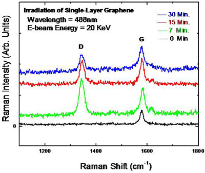
| Raman spectrum of graphene. Note the rapid rise of the disorder D peak in graphene spectrum after only few minutes of electron beam irradiation. The appearance of D peak indicates the disorder in the crystal lattice induced by the irradiation. (Image: Dr. Balandin and D. Teweldebrhan, UC Riverside) | |
| "The micro-Raman spectroscopy of graphene layers, carried out after each electron-beam irradiation step, indicates that graphene transforms to the nanocrystalline, and then to amorphous form," Balandin explains to Nanowerk. "The latter means that graphene crystalline lattice, with the long-rage ordering of atoms, first becomes polycrystalline, where the ordering is preserved only within small grains, and then transforms to a completely disordered amorphous state, which is characterized by poor electrical properties." | |
| The results of this latest work by Balandin, who leads the Nano-Device Laboratory (NDL) at the Department of Electrical Engineering and chairs the newly established Materials Science and Engineering Program at UCR, was recently published in Applied Physics Letters ("Modification of graphene properties due to electron-beam irradiation"). | |
 |
|
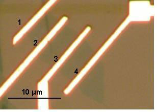
| Optical microscopy image of graphene layer with multiple contacts for measuring graphene's electrical resistance. (Image: Dr. Balandin and G. Liu, UC Riverside) | |
| "The motivation for this work" says Balandin, "was our desire to understand what happens with a graphene device when we want to have a better look at it with the help of scanning electron microscope. It turns out one can deteriorate or even destroy the device just by looking at it. The irradiation dose required for damaging graphene is smaller than that for carbon nanotubes. This is possibly due to graphene?s flat geometry, which makes it more susceptible to the electron flux." | |
| The results reported by the UCR scientists have important implications for graphene characterization and device fabrication which rely on the electron microscopy and FIB processing. | |
| Balandin points out that the importance of these findings is two-fold: On one hand, it has to be communicated to graphene researchers that even small electron beam irradiation doses, which they might use while imaging graphene flakes, deteriorate graphene's transport properties. On the other hand, it opens up the possibility of a new fabrication method for graphene devices through electron-beam irradiation. | |
| According to Balandin, the news is not necessarily negative. "We can now use electron beam irradiation to form electrically insulating regions and, in a sense, cut graphene flakes. The knowledge of the exact irradiation doses that are safe for graphene is also valuable information. Those applications of graphene which require radiation hardness would have to rely on protective coatings on top of graphene layers." | |
 By
Michael
Berger
– Michael is author of three books by the Royal Society of Chemistry:
Nano-Society: Pushing the Boundaries of Technology,
Nanotechnology: The Future is Tiny, and
Nanoengineering: The Skills and Tools Making Technology Invisible
Copyright ©
Nanowerk LLC
By
Michael
Berger
– Michael is author of three books by the Royal Society of Chemistry:
Nano-Society: Pushing the Boundaries of Technology,
Nanotechnology: The Future is Tiny, and
Nanoengineering: The Skills and Tools Making Technology Invisible
Copyright ©
Nanowerk LLC
|
|
Become a Spotlight guest author! Join our large and growing group of guest contributors. Have you just published a scientific paper or have other exciting developments to share with the nanotechnology community? Here is how to publish on nanowerk.com.