| Posted: Jan 24, 2012 |
Fabricating nanodevices with automated nanomanipulation (w/video) |
| (Nanowerk Spotlight) A field effect transistor (FET) is a type of transistor that relies on an electric field to control the shape and hence the conductivity of a 'channel' in a semiconductor material. In 2005 it was shown in a series of experiments that a silicon nanowire can be used as the source-drain channel in FETs (see paper in Nature Biotechnology: "Multiplexed electrical detection of cancer markers with nanowire sensor arrays"). Essentially, the binding of the biomolecule to the receptor behaves as a field effect – it changes the surface charge profile and the surface potential. The conductance and the I-V characteristics of the nanowire can therefore be used to characterize biomolecular binding (read more here in a previous Nanowerk Spotlight: "Amplifying biomolecular signals with nanoscale field effect transistors"). |
| Fabrication conditions for nano-FETs have to meet very high requirements in order for these transistors to be used reliably as ultrasensitive and label-free molecular sensors in medical and environmental applications. Current fabrication routes for silicon-nanowire sensor construction involve high-cost, high-complexity – and often low-yield – top-down techniques such as e-beam lithography and focused ion beam. |
| An alternative, and lower-cost, fabrication method is the use of pre-synthesized nanotubes or nanowires that are integrated into microstructures to form nano-FET sensors. The problem here, though, is the challenge to precisely control the fabrication parameters in order for the sensor devices to show only minimal to no variation in sensitivity. |
| "Many research groups have developed techniques for assembling nanoscale building blocks, such as carbon nanotubes and semiconducting nanowires, into functional electronic circuits," Yu Sun, an Associate Professor in the Department of Mechanical and Industrial Engineering, Institute of Biomaterials and Biomedical Engineering, and Department of Electrical and Computer Engineering at the University of Toronto, tells Nanowerk. "This bottom-up approach overcomes a number of limitations faced by established top-down fabrication techniques, and may be the key to continued miniaturization through the next decade. However, previously developed techniques for assembling nanoscale structures on the wafer scale rely on probabilistic means and are therefore unable to precisely control the number of nanotubes or nanowires incorporated into each device." |
| Now, Sun and his team at the Advanced Micro and Nanosystems Laboratory have developed an automated vision-based nanomanipulation technique that, when used in conjunction with existing large-scale nano-assembly methods, is capable of precisely controlling the number of nanowires incorporated into each device. |
| Reporting their findings in the January 17, 2012 online edition of Nanotechnology ("Automated nanomanipulation for nanodevice construction"), the team developed an automated visual serving algorithm for physically removing individual nanowires from an array of multi-nanowire transistor devices. |
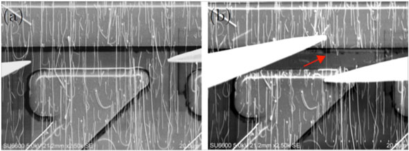 |
| Fig: (a)(b) Before and after nanomanipulation removal of nanowires between source and drain electrodes. (Images: Advanced Micro and Nanosystems Laboratory, University of Toronto) |
| "The batch microfabrication process we used is wafer-scale but has an uncontrolled number of bridging nanowires that also have significantly varying diameters," explains Yanliang Zhang, a postdoctoral fellow in Sun's group at the time of this work and the paper's first author. "Nanorobotic selective nanowire removal, despite being a serial process, permits precision control of the number and diameter of nanowires. Experimental results demonstrate that the nanorobotic system has a nano-FET device post-processing success rate of 95% (versus 48.3% for manual nanomanipulation) and has a speed of 1 min/device (versus 10.3 min/device). |
| In their work, the University of Toronto team used previously reported batch fabrication methods to fabricate arrays of nanowire transistors and load them into a scanning electron microscope (SEM) equipped with a nanomanipulation system. |
| "Although large arrays of devices can be manufactured in this manner, individual devices within the array had different numbers of nanowires and thus exhibited large performance variations due to the random nature of this manufacturing process" says Zhang. "By implementing a nanomanipulation post-fabrication process, we were able to reliably and efficiently specify the number and quality of nanowires incorporated into each device." |
| This nanomanipulation process consisted of a number of steps including visual recognition of individual nanowires and contact electrodes; classification and selection of nanowires to be kept and removed; nanoprobe path planning and visually controlled probe-substrate contact detection; nanowire removal; and finally device characterization. |
| Watch a video of the nanomanipulation process that shows the nanowire selection and removal for nano-FET sensor construction. (Credit: Advanced Micro and Nanosystems Laboratory, University of Toronto) |
| Using this technique, the team demonstrated the ability to efficiently and reliably control the number and diameters of nanowires incorporated into each device. |
| Sun notes that this technique enables precise and reliable control over individual nanoscale building blocks and offers the possibility of reasonably large-scale manufacturing of nano devices via bottom-up assembly of pre-synthesized nanostructures. |
 By
Michael
Berger
– Michael is author of four books by the Royal Society of Chemistry:
Nano-Society: Pushing the Boundaries of Technology (2009),
Nanotechnology: The Future is Tiny (2016),
Nanoengineering: The Skills and Tools Making Technology Invisible (2019), and
Waste not! How Nanotechnologies Can Increase Efficiencies Throughout Society (2025)
Copyright ©
Nanowerk LLC
By
Michael
Berger
– Michael is author of four books by the Royal Society of Chemistry:
Nano-Society: Pushing the Boundaries of Technology (2009),
Nanotechnology: The Future is Tiny (2016),
Nanoengineering: The Skills and Tools Making Technology Invisible (2019), and
Waste not! How Nanotechnologies Can Increase Efficiencies Throughout Society (2025)
Copyright ©
Nanowerk LLC
|

Become a Spotlight guest author! Join our large and growing group of guest contributors. Have you just published a scientific paper or have other exciting developments to share with the nanotechnology community? Here is how to publish on nanowerk.com. |
