| Posted: Nov 04, 2014 | |
The photothermal response of nano-devices: Electrons rolling 'uphill' in a carbon nanotube |
|
| (Nanowerk Spotlight) Semiconducting carbon nanotubes have outstanding electrical and optical properties. This has allowed for engineering device prototypes showing great potential for applications such as photodetectors and solar cells. However, any path towards industrial maturity requires a detailed understanding of the fundamental mechanisms governing the process of photocurrent generation. | |
| There has been a long debate in the nanotube community regarding the photocurrent generation mechanisms in individual nanotube devices. In early optoelectronic studies with single-walled carbon nanotubes, the interpretation of photocurrent was mostly based on photovoltaic mechanisms. | |
| The importance of photothermal effects has been suggested in the context of measurements of bulk single-walled carbon nanotube (SWCNT) films and, very recently, work on graphene and individual metallic SWCNTs has emphasized the importance of photothermal mechanisms in materials with no or small bandgaps. | |
| The question of the role of photothermal mechanisms in larger bandgap semiconducting nanotubes has been studied recently but reported contradictory results, leaving the understanding of fundamental mechanisms underlying photocurrent generation in semiconducting nanotubes unclear. | |
| In new work, published in a recent edition of Nature Communications ("Identifying signatures of photothermal current in a double-gated semiconducting nanotube"), a team led by Prof. Gary Steele at TU Delft, use the extra tunability of a double-gated device to conclusively demonstrate that strong photothermal effects are present in carbon nanotube devices. | |
 |
|
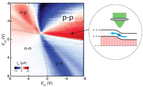
| A 2D map of the measured photocurrent (IPC) versus two local split gate voltages for the laser spot located in the middle of the suspended nanotube. The inset highlights a region where electrons are traveling 'uphill'. | |
| The study addresses the fundamental understanding of how photocurrent is generated in carbon nanotubes. This basic knowledge is crucial for the development of nanotube optoelectronic devices, and also provides a clear framework for understanding photocurrent spectroscopy not only in carbon nanotubes, but also in other devices such as graphene and semiconducting nanowires. | |
| "In our study, we designed devices with ultra-clean suspended semiconducting carbon nanotubes along which the local doping profile can be tuned using two split gates placed about 1 micron below the nanotubes," Dr. Gilles Buchs, a researcher at the Centre Suisse d’Electronique et de Microtechnique (CSEM), tells Nanowerk. "This technique – called electrostatic doping – allows for the design of p-n junctions (see: "Imaging the formation of a p-n junction in a suspended carbon nanotube with scanning photocurrent microscopy") which are elements at the heart of solar cells and many types of photodetectors." | |
| In order to study the photocurrent generation mechanisms of the devices fabricated by Dr. Salvatore Bagiante from the Paul Scherrer Institute, the team used a technique called scanning photocurrent microscopy where a diffraction-limited, continuous wave laser spot is scanned across the device surface while the photocurrent signal and the reflected light intensity are recorded simultaneously in order to determine the absolute position of the detected photocurrent features. | |
| The researchers acknowledge Prof. Val Zwiller from TU Delft for experimental support. | |
| "By placing the laser spot at the center of a suspended nanotube and recording the photocurrent for the entire gate voltage space, we obtained a two-dimensional (2D) photocurrent map showing interesting patterns from which we could deduce that for specific gate voltages, the electrons are travelling 'uphill', i.e. against the electric field," explains Buchs. "Such remarkable behavior cannot be explained by the photovoltaic effect, which is usually the main dominant mechanism for photocurrent generation in conventional solar cells." | |
| "In the case of our device, such a counter-intuitive behavior can be understood through a subtle thermoelectric effect," notes Steele. "Indeed, it can be shown that for the typical light intensity used in this work, the laser spot heats up the nanotube locally by about 1 K above the contacts' temperature and the resulting thermal gradient creates a local electromotive force which will act on carriers present in the nanotube through the Seebeck effect. This force is proportional to the Seebeck coefficient, which is a measure of the magnitude of the electromotive voltage in response to the temperature difference across the material, and the local thermal gradient." | |
| The Seebeck coefficient is positive for holes (p doping) and negative for electrons (n doping) and therefore electrons and holes are swept in opposite directions. | |
| As the team points out, for semiconducting nanotubes, it can be shown that the amplitude of the Seebeck coefficient has a maximum value for carrier energies close to the bandgap edges and is decaying when the energy is pulling away from the bandgap. | |
 |
|
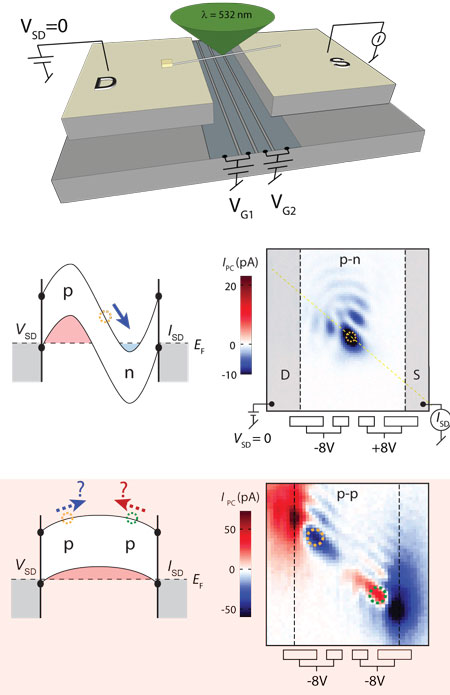
| Top: Schematic of the device. Middle and Bottom: Qualitative band diagrams and photocurrent images measured for p–n, and p–p doping configurations, respectively. The sign of the photocurrent corresponds to the conventional flow notation (red: positive, blue: negative) and the arrows on the band diagrams are oriented according to the electron flow notation. The bottom panel illustrates the dominant photothermal mechanism observed in the p–p configuration where electrons are flowing ‘uphill’. | |
| "Using a simple thermocouple model, we show that this key fact has as a consequence that for two portions of the nanotube both doped n or p but with different levels, the resulting current is flowing against the induced electric field," says Buchs. "In this way, our technique allowed to demonstrate that in semiconducting nanotube devices, both photovoltaic and photothermal current are induced when the nanotube is optically excited." | |
| From their 2D photocurrent map, the researchers also demonstrate that – although both photovoltaic and photothermal currents are always present in the nanotube device – their dominant or non-dominant character strongly depends on the properties of the metal contacts. | |
| In their device, strong signatures for photothermal current show up for the p-p doping configuration and almost all photocurrent signal is suppressed for the n-n region. This is due to the fact that the Fermi level of the contacts is quasi aligned with the valence band edge of the nanotube, thus creating large Schottky barriers for electrons, preventing them to flow in the nanotube for a n-doping configuration. | |
| Such findings advance the field of carbon nanotube and more generally nano-carbon based optoelectronics with a better understanding of the photocurrent generation mechanisms, allowing for more control in future devices such as solar cells for example. | |
| In addition, the results are very important for designing better controlled and potentially more efficient solar cells or photodetectors based on carbon nanotubes and more generally nano-carbon materials. | |
| "In the context of carbon nanotubes, a clear understanding of these phenomena opens up the potential for using optical techniques for identifying the 'flavor' (chirality) of carbon nanotubes in devices, an open problem that limits fundamental research with these devices," concludes Buchs. "The thermoelectric effect itself is also potentially useful for generating electricity from waste heat in things like nanodevices and microprocessors: the tunable nature of the thermoelectric effect we show in our work could potentially be applied to optimize such energy-harvesting devices in the future." | |
 By
Michael
Berger
– Michael is author of three books by the Royal Society of Chemistry:
Nano-Society: Pushing the Boundaries of Technology,
Nanotechnology: The Future is Tiny, and
Nanoengineering: The Skills and Tools Making Technology Invisible
Copyright ©
Nanowerk LLC
By
Michael
Berger
– Michael is author of three books by the Royal Society of Chemistry:
Nano-Society: Pushing the Boundaries of Technology,
Nanotechnology: The Future is Tiny, and
Nanoengineering: The Skills and Tools Making Technology Invisible
Copyright ©
Nanowerk LLC
|
|
|
Become a Spotlight guest author! Join our large and growing group of guest contributors. Have you just published a scientific paper or have other exciting developments to share with the nanotechnology community? Here is how to publish on nanowerk.com. |
|