Showing Spotlights 65 - 72 of 110 in category All (newest first):
 Since its invention in 1986 by Binnig, Quate, and Gerber, the atomic force microscope (AFM) has become an indispensable tool for investigators in the physical, materials, and biological sciences. The AFM quickly gained acceptance in these fields due to its ability to capture topographical maps of surfaces in either air or liquid with sub-angstrom and nanometer resolution. This Application Note briefly describes the basics of both optical and atomic force microscopy, followed by a discussion of some of the technical challenges of integrating these two distinct imaging modalities. In certain cases, the benefits and disadvantages of different approaches to design and integration are discussed. Lastly, a few examples of successful application of these combined imaging modalities are presented.
Dec 16th, 2009
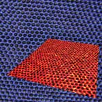
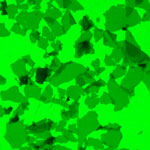 Graphene based sheets such as pristine graphene, graphene oxide, or reduced graphene oxide are basically single atomic layers of carbon network. They are the world's thinnest materials. A general visualization method that allows quick observation of these sheets would be highly desirable as it can greatly facilitate sample evaluation and manipulation, and provide immediate feedback to improve synthesis and processing strategies. Current imaging techniques for observing graphene based sheets include atomic force microscopy, transmission electron microscopy, scanning electron microscopy and optical microscopy. Some of these techniques are rather low-throughput. And all the current techniques require the use of special types of substrates. This greatly limits the capability to study these materials. Researchers from Northwestern University have now reported a new method, namely fluorescence quenching microscopy, for visualizing graphene-based sheets.
Dec 14th, 2009
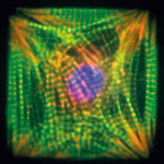
 Single molecule detection requires tools that have the detection sensitivity at the scale of single molecules. This could mean a spatial resolution requirement of only a few nanometers especially if the precise location of the molecule needs to be mapped. Researchers have already developed spectroscopic techniques capable of physical and chemical mapping on a nanometer scale. Researchers in Italy have now reported the design, fabrication and application of a photonic-plasmonic device that is fully compatible with atomic force microscopy and Raman spectroscopy - an approach that is novel in both scientific and technological aspects. The device consists of a two-dimensional dielectric photonic crystal cavity patterned on an AFM cantilever, together with a tapered silver waveguide placed at the center of the cavity.
Nov 24th, 2009
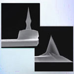
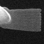
 Many of today's high-tech products rely on nano-level functional structures, and in products such as mobile phones, integrated circuits and glasses they have already become commonplace. But with increasing demands on products and their quality, tiny structures and the ability to evaluate them are also becoming decisive factors for the production of everyday products. The experience of a ball-point pen maker shows how atomic force microscopy enables highly accurate quality control during manufacturing, eliminating entire production steps in the process. Everyone has had to contend with scratchy or messy ball-point pens, but not everyone knows that often this malfunction is the result of a manufacturing error: smooth writing depends largely on the roughness of the sphere at the tip of the pen. Its roughness needs to lie in a well-defined interval: too rough, and the pen leaks; too smooth, and it scratches and fails to transport enough ink. The roughness of this little sphere thus becomes the decisive quality indicator of the entire writing apparatus.
Nov 18th, 2009
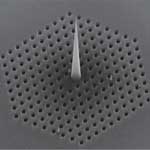
 Over the past decade, Atomic Force/Scanning Probe Microscopy (AFM/SPM) has emerged as the leading tool for investigations at the nanoscale - doing everything from imaging, to compositional differentiation, to explorations of molecular forces. But aside from some interesting tweaks, add-ons and repackaging, the field has seen no fundamentally new instruments for several years. For the extremely high-resolution AFM/SPMs, there has literally been no completely new microscope for well over a decade. Enter the new Cypher AFM. Cypher was designed from the ground up with a host of new features and unmatched performance enabled by its revolutionary new design.
Nov 12th, 2009
 In today's addition to our Application Note series we are looking at the future of electronics and the implications for research instrumentation. We are showing two examples of atomic force microscope (AFM) applications employed in this research. Current CMOS (complementary metal-oxide-semiconductor) technology used for making integrated circuits is constantly being scaled down. These devices will reach their ultimate physical limits in 10 to 15 years. As chip structures - which currently already have reached nanoscale dimensions - continue to shrink below the 20 nanometer mark, ever more complex challenges arise and scaling appears not to be economically feasible any more. And below 10 nm, the fundamental physical limits of CMOS technology will be reached. Researchers are therefore exploring novel concepts for future nanoelectronic devices.
Nov 2nd, 2009
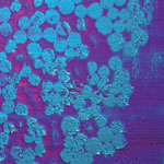
 Traditional techniques in cell biology involve chemical or pharmaceutical treatments of entire cells; however, in many cases it would be advantageous to target a single organelle or other structure within a cell without damaging overall cell structure. If scientists could inject a drug into a chosen organelle within the cell, or even destroy, extract or isolate the whole organelle without significantly harming the cell itself, new insight could be gained into the inner workings of the cell. In recent years, techniques have been developed which allow the manipulation of the individual nanoscale structures within biological cells. This manipulation, or 'nanosurgery', has the potential to provide new insight into the internal structure and dynamics of cells. Nanosurgical methods have been developed to target the cell's internal organelles, the cell membrane, and the structural protein filaments within the cell.
Oct 30th, 2009
 Today, in our Application Note series, we are covering Scanning Thermal Microscopy (SThM) - an atomic force microscopy (AFM) imaging mode that maps changes in thermal conductivity across a sample's surface. Similar to other modes that measure material properties, SThM data is acquired simultaneously with topographic data. The SThM mode is made possible by replacing the standard contact mode cantilever with a nanofabricated thermal probe with a resistive element near the apex of the probe tip. This resistor is incorporated into one leg of a Wheatstone bridge circuit, which allows the system to monitor resistance. This resistance correlates with temperature at the end of the probe, and the Wheatstone bridge may be configured to either monitor the temperature of a sample or to qualitatively map the thermal conductivity of the sample.
Oct 8th, 2009
 Subscribe to our Nanotechnology Spotlight feed