Showing Spotlights 57 - 64 of 110 in category All (newest first):
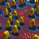 Plastic solar cells are emerging as alternative energy sources for the future because of their potential for cheap roll-to-roll printing, ease of processing, light-weight and flexibility. However, their current performance is still low for practical applications which partially originate from the poor understanding of device physics and nanoscale morphology of the photoactive layer. Photoconductive atomic force microscopy (pcAFM)is a powerful characterization tool to better understand the complex optoelectronic and morphological phenomena of organic solar cells at the nanoscale. This article briefly described the applicability of the pcAFM technique for analyzing solution-processed, polymer and small molecule bulk heterojunction solar cells. Due to the nature of charge generation, transport and collection occurring at the nanometer scale, the useful information on device operation can be lost from macroscopic measurements.
Sep 15th, 2010
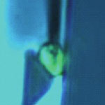 An intriguing novel approach to extract the energy from the photosynthetic conversion process has been demonstrated by researchers at Stanford and Yonsei Universities. They have inserted ultrasharp gold nanoelectrodes into living algae cells and extracted electrons, thereby harnessing an - albeit very tiny - electrical current. This is electricity production that doesn't release carbon into the atmosphere. The results demonstrate the feasibility of collecting high-energy electrons in steps of the photosynthetic electron transport chain and prior to the downstream processes associated with energy loss. In addition, the system allows direct monitoring of specific charge transfer reactions in live cells, leading to broad applications for investigating developmental processes and the responses of cells and organelles to light and chemical stimuli.
May 3rd, 2010
 Most of the material properties investigated by atomic force microscopy are acquired by processing the deflection signal of the cantilever, which is applied to Electrostatic Force Microscopy (EFM) measurements as well. For EFM, the sample surface properties would be electrical properties and the interaction force will be the electrostatic force between the biased tip and the sample. Electrostatic Force Microscopy maps electric properties on a sample surface by measuring the electrostatic force between the surface and a biased AFM cantilever. EFM applies a voltage between the tip and the sample while the cantilever hovers above the surface, not touching it. The cantilever deflects when it scans over static charges.
Apr 21st, 2010
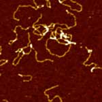 Imaging soft biological samples in liquid with Atomic Force Microscope has long stood as a very challenging task. Until recently, most of the works in this field has been carried out in tapping mode AFM, during which the cantilever driven by a piezoelectric actuator vibrates in the vicinity of the cantilever's resonance frequency, and briefly touches the sample surface at the bottom of each vibration cycle, resulting in a decrease of its oscillation amplitude. By keeping such amplitude at a preset value using feedback control, a topographic image of the sample surface is obtained. However, stable, high-resolution imaging of very fragile and sensitive biological samples such as live cells or individual proteins is not trivial in tapping mode due to potential sample distortion or even damage during the brief contact between the AFM tip and sample surface at the end of each oscillation cycle. The XE-series AFM with Crosstalk Elimination and high force Z-scanner has successfully solved these problems.
Mar 9th, 2010
 Solar cells, or photovoltaic cells, are used to convert sunlight into electrical power. As traditional power sources grow scarce, other forms of producing electrical power are gaining firm footing in the power supply mix. Solar cells are already widely used in a variety of applications - from spacecraft, to small portable devices, to farm installations, to roadway signs. As energy prices increase, public demand for solar power has surged. In order to meet the longevity, yield, and price requirements of consumers and industry, public and private sector research has increased dramatically. While traditional tools are helpful to investigate and improve solar cells, AFM/SPM offers metrology, topography and roughness analysis at much higher resolution than with optical techniques.
Mar 2nd, 2010
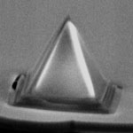 Many nanotechnology applications are plagued by very poor wear resistance of device components at the nanoscale. Gears, bearings, and liquid lubricants can reduce friction in the macroscopic world, but the origins of friction for small devices such as micro- or nanoelectromechanical systems require other solutions. Despite the unprecedented accuracy by which these devices are nowadays designed and fabricated, their enormous surface-volume ratio leads to severe friction and wear issues, which dramatically reduce their applicability and lifetime. Although there is a significant amount of research work going on in the area of nanoscale friction, at present there is much less research conducted on nanoscale wear. Researchers have now demonstrated extremely low wear rates at the nanoscale, representing a technological breakthrough for numerous applications in emerging fields such as nanolithography, nanometrology, and nanomanufacturing.
Feb 15th, 2010
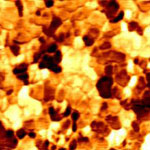
 In characterizing materials, especially live biological specimen such as cells, it is important not only to be able to explore the surface but also any subsurface structures and properties - without damaging or destroying the sample and for hard and soft materials alike. For example, many synthesized nanoparticles can readily get inside a cell. Therefore studying the cell surface, while useful, can provide little or no knowledge about the particles hidden in the interior of the cell. Another example is the detection of nanoscale defects in nanofabricated structures such as those made by electron beam lithography; or the detection of embedded cracks and voids in nanocomposite materials. Researchers have now shown that an atomic force microscope can obtain a range of surface and subsurface information by making use of the nonlinear nanomechanical coupling between the probe and the sample.
Jan 18th, 2010
 After two decades of evolution, Atomic Force Microscopy (AFM) has established its strong existence in the material science research field with its nanoscale resolution. Of the systems out in the market, the innovative XE-AFMs have overcome the non-linearity and non-orthogonality problems associated with traditional piezoelectric tube based AFMs. Active in both research and industrial applications including hard-disk, microchip fabrication, and quality control, the XE series has been widely adopted in the nanometrology field. The most recent addition to the XE family, the XE-Bio, has integrated the high resolution of AFM imaging and non-invasiveness capabilities Scanning Ion Conductance Microscopy with the versatility of advanced optical microscopy techniques such as scanning confocal microscopy, FRET and TIRF. Therefore, the XE-Bio is able to correlate the highest possible spatial resolution with dynamic functionality studies on live biological samples.
Jan 7th, 2010
 Subscribe to our Nanotechnology Spotlight feed