Showing Spotlights 41 - 48 of 110 in category All (newest first):
 Optical tweezers offer researchers the chance to perform precise force sensing in a fluid environment. This could help to give clarity to some of the picoNewton forces that govern fundamental processes in the cell. However, currently the use of tweezers to probe biological, samples requires either direct irradiation with a laser, or the use of a tool or proxy to exert or sense very small forces. There are many instances when exposing samples to high intensity laser light is less than ideal - typically this is within a biological context. Researchers have now have shown that optical tweezers can be combined with naturally derived algae to create a stable nanoscale optical force sensor. This may enable other groups to utilize this technique to probe key force interactions that occur at the lowest end of the nanoscale force regime.
Nov 15th, 2012
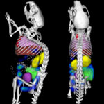 One of the key issues in the development of novel nanomedicines is the ability to track nanoscale drug carriers inside the body to evaluate where they go and how they get there. Virtually all previous preclinical studies in this area of research rely on 2D Fluorescence Reflectance Imaging (FRI). Given the limitation of 2D FRI in not being able to detect the fluorescence in deep-seated organs and tissues, 3D Fluorescence Molecular Tomography (3D FMT) emerged as an alternative. However, the lack of anatomical information was an important barrier hindering the routine use of standard 3D FMT for in vivo imaging of nanomedicines. Researchers have now developed a hybrid CT-FMT-based imaging protocol to enable more meaningful and more quantitative in vivo analyses.
Nov 13th, 2012
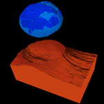 Nanostructured surfaces with special wetting properties can not only efficiently repel or attract liquids like water and oils but can also prevent formation of biofilms, ice, and other detrimental crystals. Such super- and ultrahydrophobic surfaces also hold the promise of significantly improving performance of condensers, which could boost the efficiency of most power plants in the world. A critical part of designing such surfaces is 'seeing' how water and other liquids interact when in contact with them. Since these surfaces are made of nanostructures, scientists need to use an electron microscope to image these interactions. In new work, researchers have developed a method for directly imaging such interfacial regions with previously unattainable nanoscale resolution.
Oct 24th, 2012
 Doping, the process of adding impurity atoms to semiconductors to provide free carriers for conduction, has been pivotal to microelectronics since its early stages. In particular doping germanium at high concentrations to make it highly conductive is the subject of intense research, because it lies at the heart of novel developments in integrated silicon-compatible lasers and quantum information processing devices. Researchers have now demonstrated a method to densely pack dopant molecules on the germanium surface, which then self-organize to form molecular patterns with one phosphorus dopant atom every two germanium atoms. The key finding is that when you deposit phosphine molecules on a germanium surface, they naturally form molecular patterns with one phosphorus atom every two germanium atoms that densely pack the surface.
Aug 14th, 2012
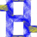 Researchers have demonstrated that electrons in nanoscale networks can behave like car drivers in congested cities. Traffic planners are sometimes faced with a rather counter-intuitive observation - adding a new road to a congested road network can lead to a deterioration of the overall traffic situation, i.e. longer trip times for individual road users. Or, in reverse, blocking certain streets in a complex road network can counter-intuitively reduce congestion. This has become known as the Braess paradox. Researchers have now applied the concept of the Braess paradox to the quantum world. By combining quantum simulations of a model system and scanning-probe experiments, they have shown that an analogue of the Braess paradox can occur in mesoscopic semiconductor networks, where electron transport is governed by quantum mechanics. The paradox manifests itself by an increase of the conductance network when one arm in the network is partially blocked in a controlled manner.
Feb 21st, 2012
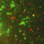 In nanomedicine, nanoparticles are used as vehicles for efficiently delivering therapeutic nucleic acids, such as disease-fighting genes and small interfering RNA (siRNA) molecules, into cells. But getting nanomedicines to their target sites inside cells is not the only challenge. It also is necessary to assess the intracellular processing of nanomedicines and the efficacy of their payload delivery - a task that is not exactly trivial given the complexity and dynamics of the mechanisms of endocytosis and intracellular trafficking. Researchers are therefore trying to develop robust and reliable tools to characterize and evaluate the intracellular processing of administered nanomedicines. As part of this effort, scientists have now introduced a quantitative approach to study live-cell endosomal colocalization dynamics of nanomedicines for gene delivery, based on single-particle tracking and trajectory-correlation.
Nov 21st, 2011
 Uncertainty evaluation is an often overlooked factor in many AFM material property measurement work - nevertheless it is critical for obtaining truly quantitative measurements. The atomic force microscope is used extensively for measuring the material properties of nanomaterials with nanometer resolution, unfortunately there is a lack of standards and uncertainty quantification in these measurements. Other fields, such as six sigma standards in industry and beam corrections in scanning electron microscopy, have developed thorough methods for quantifying the uncertainty in a given measurement, model, or system. Broadly speaking these methods can be classified as uncertainty quantification. Without applying the methods of uncertainty quantification to AFM measurements it is impossible to say if the measurements are accurate within 5% or 100%.
Nov 11th, 2011
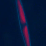
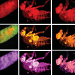 Fruit flies (Drosophila melanogaster) are the workhorses in countless biomedical research laboratories around the world. The bioimaging of live specimens, ideally through all the stages of the fruit fly life cycle, is a tricky and often complicated undertaking. Researchers in India have now developed a relatively simple way to introduce fluorescent nanomaterials into fruit flies: They prepared carbon nanoparticles from wood waste and added them to the flies' food supply. The fluorescent fruit flies showed no toxic effects - upon withdrawal of the nanoparticles from their food, they excreted the fluorescing material and continued to proliferate to the next generation, demonstrating a return to their normal lives.
Nov 8th, 2011
 Subscribe to our Nanotechnology Spotlight feed