Low-dimensional Materials: 0D, 1D, and 2D Nanostructures Explained
What are Low-dimensional Materials?
In one sentence: Low-dimensional materials are solids in which one, two, or all three external dimensions are reduced to length scales that confine electrons, phonons, or photons, so that quantum confinement, surface effects, and a reshaped electronic density of states produce properties unavailable in the corresponding bulk material.
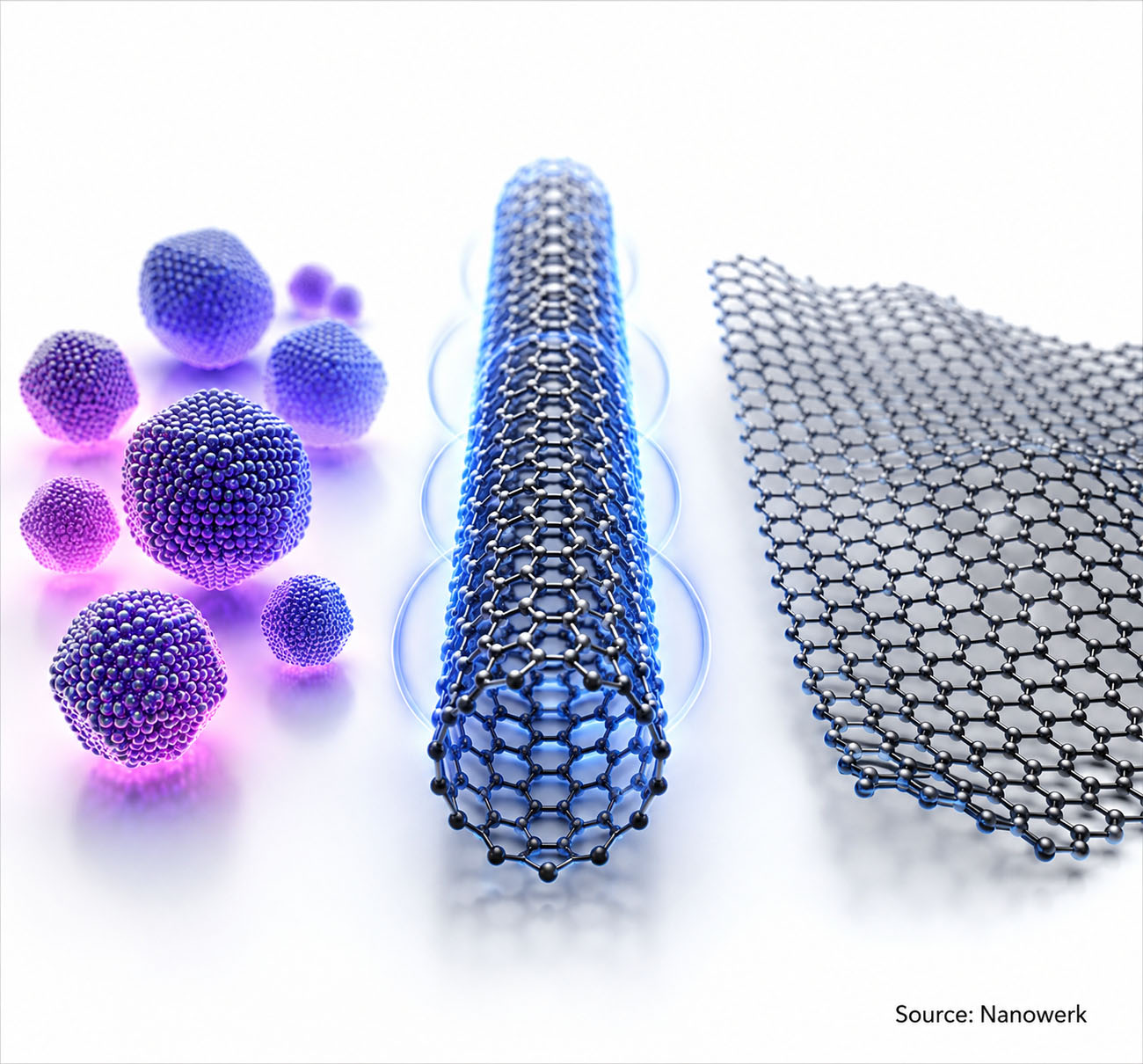
The classification used across condensed-matter physics, materials science, and nanotechnology is based on the number of dimensions in which the material extends macroscopically. Three-dimensional (3D) bulk solids extend in all directions and serve as the reference. Two-dimensional (2D) materials are sheet-like, with thickness of one to a few atomic layers and lateral extent of micrometers or more. One-dimensional (1D) materials are filament-like, with diameter in the nanoscale but length many orders of magnitude greater. Zero-dimensional (0D) materials are particle-like, confined in all three directions to a few to tens of nanometers. The defining feature is geometry rather than chemistry: the same element, such as carbon, gives a 0D fullerene, a 1D nanotube, and a 2D graphene sheet, each with markedly different electronic and mechanical behavior.
The modern field predates graphene by decades. Quantum wells were demonstrated by molecular beam epitaxy in the 1970s, fullerenes were isolated in 1985, carbon nanotubes were characterized by Sumio Iijima in 1991, and colloidal semiconductor nanocrystals were widely studied through the 1990s. The 2004 isolation of graphene by Andre Geim and Konstantin Novoselov, followed in 2005 by the demonstration that many other layered crystals could be reduced to monolayers, opened the modern era of van der Waals materials. Publication output on 2D materials has grown from a niche literature in the early 2000s to a major research field with many thousands of papers published annually.
Key takeaways:
- Low-dimensional materials are classified by how many dimensions extend beyond the nanoscale: 0D (all confined), 1D (one free), 2D (two free).
- The transition from 3D to lower dimensionality reshapes the electronic density of states, introduces quantum confinement, and raises the surface-to-volume ratio.
- Representative classes include quantum dots and nanoparticles (0D); nanowires, nanotubes, and nanofibers (1D); and graphene, transition metal dichalcogenides, MXenes, and other van der Waals monolayers (2D).
- Heterostructures combining different dimensionalities extend the design space and provide platforms for electronics, photonics, catalysis, sensing, and energy storage.
How Dimensionality Changes Electronic and Physical Properties
The most important consequence of reducing dimensions is the change in the electronic density of states (DOS). In a 3D bulk metal or semiconductor with simple parabolic bands, the DOS varies smoothly with energy. In a 2D system it becomes a series of step functions, one for each confined subband. In a 1D wire it develops sharp van Hove singularities at each subband edge. In a 0D quantum dot, the DOS collapses to a set of discrete delta-function-like levels, much like the energy levels of an isolated atom, which is why semiconductor quantum dots are sometimes called artificial atoms. These changes reshape optical absorption, carrier transport, magnetism, and chemical reactivity in ways that cannot be reproduced in bulk samples of the same composition.
The crossover from bulk to low-dimensional behavior is set by characteristic length scales. Quantum confinement appears when one or more dimensions shrinks below the de Broglie wavelength of charge carriers, typically a few to tens of nanometers in semiconductors. Below this scale the bandgap widens and shifts to higher energy, an effect that lets the emission color of a quantum dot be tuned by particle size alone. In thin films the same physics produces the discrete subbands exploited in high-electron-mobility transistors and quantum cascade lasers, and at smaller scales it underlies the family of quantum size effects that dominate the optical response of nanocrystals.
Surface effects scale together with confinement. The fraction of atoms residing at or near a surface rises roughly in inverse proportion to the smallest dimension, so a 5 nm nanocrystal can have a large fraction, often tens of percent, of its atoms at or near the surface, while a monolayer 2D material is essentially all surface. The resulting elevated surface-to-volume ratio drives strong catalytic activity, modified mechanical and thermal behavior, and a sensitivity to environmental adsorbates that has been turned into a basis for chemical and biological sensing. Where the smallest dimension also approaches the electron mean free path, transport becomes ballistic rather than diffusive, enabling near-ideal mobility in clean samples.
Classification of Low-dimensional Materials
The table below summarizes the standard classification based on the number of unconfined dimensions, together with representative examples and the dominant physics. Bulk 3D solids are included as the reference category against which the other classes are usually compared.
| Dimensionality | Geometry | Representative examples | Defining physics |
|---|---|---|---|
| 3D (bulk) | Extended in all directions | Conventional metals, semiconductors, insulators, polycrystalline ceramics | Continuous parabolic density of states; properties dominated by bulk band structure |
| 2D | Extended in two directions, atomic thickness in the third | Graphene, hexagonal boron nitride, transition metal dichalcogenides such as MoS2, phosphorene, MXenes | Step-like density of states, planar transport, strong sensitivity of properties to layer number |
| 1D | Extended in one direction, nanoscale cross-section | Nanowires, carbon nanotubes, nanorods, nanoribbons, nanofibers | Van Hove singularities in the density of states; anisotropic transport, often ballistic at small diameters |
| 0D | Confined in all three directions to a few to tens of nm | Semiconductor quantum dots, metal nanoclusters, fullerenes, carbon dots, graphene quantum dots | Discrete atom-like energy levels; size-tunable bandgap and emission |
Although the categories are clean in theory, real materials often straddle them. A short, thick nanowire behaves as 1D for charge transport but as 0D for its lowest excitonic states; a 2D sheet whose lateral dimension is reduced to a nanoribbon develops 1D-like edge states; and a 0D nanocrystal grown anisotropically into a platelet shows mixed 0D and 2D character. The classification is most useful as a guide to which confinement direction dominates, rather than as a strict boundary.
Synthesis and Fabrication Approaches
Two complementary strategies are used to prepare low-dimensional materials. Bottom-up methods build the structure from atomic or molecular precursors: chemical vapor deposition grows 2D sheets and 1D filaments on a substrate, molecular beam epitaxy gives ultra-clean quantum wells and superlattices, colloidal synthesis produces uniform quantum dots, and self-assembly organizes peptides, surfactants, or block copolymers into structures with nanoscale dimensionality. Top-down methods carve nanostructures from a larger parent: the scotch-tape method isolates single 2D layers from layered crystals, liquid-phase exfoliation gives suspensions of monolayer flakes at larger scale, and lithographic patterning combined with etching defines nanowires and nanoribbons in semiconductors.
The choice depends on the target dimensionality and the requirements of the application. Atomic-scale uniformity in electronic devices usually requires epitaxial growth or careful mechanical cleavage, while solution-processed coatings, composites, and inks rely on liquid-phase exfoliation and colloidal synthesis. Many modern systems combine both: 2D monolayers grown by chemical vapor deposition on metal foils are transferred onto target substrates, and 0D nanocrystals are deposited from solution onto pre-patterned 2D channels to form composite optoelectronic devices.
Heterostructures and Mixed-Dimensional Systems
Different low-dimensional materials can be combined to make heterostructures whose properties go beyond those of any individual component. The most studied example is the van der Waals heterostructure: a stack of 2D monolayers held together by weak interlayer forces, which allows almost arbitrary combinations of materials with different electronic structures to be assembled layer by layer. Because the interlayer coupling is weak, lattice mismatch is not the constraint it is in conventional epitaxy. Twisting two layers at a controlled angle produces a moiré superlattice; at the magic angle of about 1.1° in twisted bilayer graphene, flat electronic bands appear that host correlated insulating states and unconventional superconductivity.
Mixed-dimensional architectures take this further by integrating 0D nanocrystals with 2D substrates, decorating 1D nanowires with 0D catalyst particles, or threading narrow 2D nanoribbons through 1D nanotubes. The interfaces combine the high active-site density of nanoparticles with the long-range, low-defect transport of nanowires or 2D sheets, producing photodetectors, electrocatalysts, and battery electrodes that outperform single-component systems.
Applications
Low-dimensional materials underpin a broad range of present and emerging technologies. 0D quantum dots provide narrow, size-tunable emission used in display backlights, quantum dot light-emitting diodes, lasers, and biological imaging probes. 1D nanowires and nanotubes serve as transistor channels at sub-10 nm gate lengths, as photovoltaic absorbers, transparent electrodes, gas and biochemical sensors, and as electrode materials in lithium-ion and lithium-sulfur batteries. 2D materials such as graphene and transition metal dichalcogenides are used in flexible and transparent electronics, photodetectors, electrocatalysts for the hydrogen evolution reaction, supercapacitor and battery electrodes, and impermeable barrier coatings. Common to most applications is that the small dimension either tunes the electronic structure through confinement or exposes a very high surface area in a fabrication-friendly geometry.
Challenges and Future Perspectives
Several persistent challenges shape the field. Scaling laboratory demonstrations to wafer-scale or industrial production without sacrificing uniformity is difficult for almost all classes. 2D monolayers grown by chemical vapor deposition over large areas typically have grain boundaries, polycrystallinity, and a finite defect density that degrade transport relative to mechanically exfoliated flakes. Forming reliable, low-resistance electrical contacts to atomically thin materials remains a major obstacle in 2D electronics. Stability also varies widely: graphene and hexagonal boron nitride are air-stable, while phosphorene and many MXenes degrade in ambient conditions and require encapsulation.
Looking forward, the field is moving toward designed combinations of dimensionalities rather than the further optimization of any single class. Twisted 2D bilayers continue to reveal strongly correlated electronic phases; mixed-dimensional heterostructures with engineered band alignments are extending the range of accessible optoelectronic functions; and integration with established silicon technology is opening hybrid devices. Computational screening combined with high-throughput synthesis is accelerating the discovery of new monolayer compositions, particularly in the magnetic, ferroelectric, and topological families.
FAQ: Low-dimensional Materials
What is the difference between low-dimensional materials and nanomaterials?
Nanomaterials is a broad umbrella that usually covers materials with at least one external, internal, or surface structural feature in the approximate 1–100 nm range, regardless of geometry. Low-dimensional materials are a subset that emphasizes dimensional confinement itself, classifying a material by how many of its dimensions remain macroscopic. In strict usage, a three-dimensional nanoporous bulk solid is a nanomaterial but not a low-dimensional material, whereas a quantum well, a nanowire, and a two-dimensional monolayer are all both.
Why are semiconductor quantum dots called artificial atoms?
In a sufficiently small semiconductor quantum dot, the electronic density of states collapses from a continuous band into a discrete set of well-defined levels, much like the orbitals of an isolated atom. The size, shape, and chemical composition of the dot tune these levels in a way that is impossible for real atoms. That tunability is what makes quantum dots attractive as building blocks for single-photon sources, qubits, and color-tuned light emitters.
Are two-dimensional materials only one atom thick?
Some of the best-known two-dimensional materials, including graphene and hexagonal boron nitride, are one atom thick. Others, such as molybdenum disulfide and many MXenes, are two to five atoms thick within a single formula-unit layer. Few-layer stacks of these materials are also commonly described as two-dimensional, since their electronic properties remain dominated by the layered structure rather than by three-dimensional bulk behavior.
Can low-dimensional materials replace silicon in electronics?
Most researchers treat low-dimensional materials as complements rather than wholesale replacements for silicon. Two-dimensional channel materials such as molybdenum disulfide are being investigated for ultra-short transistors where bulk silicon performance degrades; carbon nanotubes and silicon nanowires have demonstrated competitive transistor behavior at small dimensions; and zero-dimensional quantum dots provide optoelectronic functions outside silicon’s reach. Practical adoption depends as much on contacts, integration, and process compatibility as on intrinsic material performance.
Further Reading
Proceedings of the National Academy of Sciences, Two-dimensional atomic crystals
Nature, Van der Waals heterostructures
Nanomaterials, A Review on Low-Dimensional Nanomaterials: Nanofabrication, Characterization and Applications
Chemical Reviews, Charge Transfer from Quantum-Confined 0D, 1D, and 2D Nanocrystals
