| Posted: Mar 10, 2016 | |
Three new developments for smarter sensor chips |
|
| (Nanowerk Spotlight) Sensors have evolved from simple measuring tools to smart appliances that are connected through the internet to the cloud and to each other. At the recent ISSCC-conference, researchers from imec & Holst Centre have presented a number of remarkable developments. These may pave the way to a world where sensors assist us to drive more safely, live healthier, and make the planet more sustainable. | |
| Sensors Become the Senses of Our Environment | |
| Our environment will slowly but surely evolve into an ‘Internet of Things’, where chips and sensors are integrated invisibly in the environment to assume their manifold tasks. Think of sensors that detect the presence of individuals and adapt the light in a building accordingly, resulting in serious energy savings. Those sensors will be, in a sense, the eyes, ears, and noses of our environment. | |
| Ubiquitous sensors will make their mark in many domains—smart buildings, self-driving cars and automated industrial and logistic processes to name a few. And, essential for a more sustainable future, sensors will be of great help to tackle environmental issues. If we are able to measure the quality of air and water continuously and in a fine-grained way, and we can collect the data centrally, it may be possible to take better-directed actions, and immediately measure the results. | |
| But also in the domain of healthcare, there are great opportunities. Think of simple tools such as weighting scales, blood pressure monitors, or heart and activity monitors that will send their data (secured!) to the cloud. There, the data may be analyzed and become the basis for new services to coach patients to lead a healthier life. This type of connected healthcare is already applied on a small scale with high-risk patients. But as the technology becomes smarter and cheaper, it could serve many more. | |
 |
|
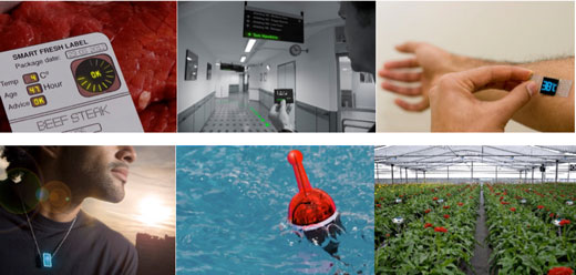
| Sensors will have an influence in many sectors. Here are some artist impressions of possible applications of integrated sensoring: smart food labeling, personal signage using LEDs, thermoflex patches, air quality necklace, water poution monitoring, plant health monitoring. | |
| TREND 1: Sensor Fusion—Combining Sensors for a Better Result | |
| Sensors won’t have an easy time. As they have to function day in, day out, they will have to leave their comfort zone and get used to highly variable temperatures, humidity, aridity, and vibrations. They will have to keep on working in harsh conditions and still deliver reliable results. | |
| One of the possibilities is sensor fusion: measuring the same physical parameter with a number of different sensors (e.g. someone’s heartbeat that can be monitored electrically, optically and even acoustically). By combining the results of the sensors and interpreting the result, it is possible to arrive at a robust and reliable result. Context awareness could also be added. For example, a sensor that ‘feels’ a person has started sleeping communicates this result to a second sensor that has the task to monitor the heart at rest so one sensor flags the ideal moment for the other sensor to start work. | |
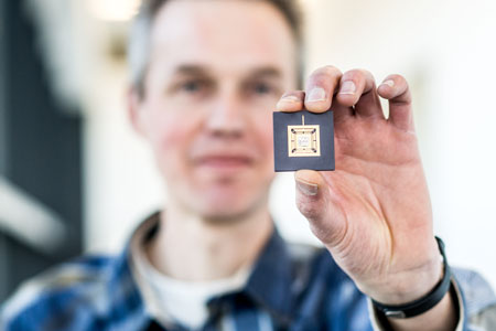
| At ISSCC, researcher Mario Konijnenburg from Holst Centre/imec presented some remarkable results. Together with a colleague, he developed a chip that is able to measure several body parameters at the same time: an electrocardiogram (ECG), bio-impedance (BIO-Z, electrical conductivity of the body revealing the composition of body tissues), galvanic skin response (GSR, changes in the electrical properties of the skin due to e.g. stress), and photoplethysmogram (PPG, changes in the blood circulation in tissues due to changing light absorption). Because these data are collected on one chip, it is perfectly possible to synchronize them and look for correlations. In this example, the combination of measurements allows for a reliable way to deduce heartbeat and heart rate variability while (relative) blood pressure can be deduced by interpreting the ECG- and PPG measurements. | |
 |
|
| Mario Konijnenburg with his multi-sensor chip. | |
| TREND 2: Local Processing: Processing Data on the Chip is Energy Efficient | |
| Data from the sensors chip are wirelessly sent to the cloud (e.g. through a smartphone or laptop). In the cloud, the data are processed and interpreted. Presently, 80% of the energy consumed by the sensors is used by the wireless link. So if the sensor has to be made more energy-efficient, it should send less data. This can be done by processing and interpreting the data partly on the sensors, only sending the results to the cloud. Of course, processing on the chip will also consume energy, so part of the researchers’ task is to find the optimal balance between on-chip processing and sending data to the cloud. | |
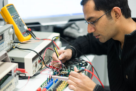
| If the sensor has to do more local processing, it will need one or more additional processing cores. Advanced chip technologies are ideal to integrate more powerful processing on an already very small chip. But, as the world is analog, we still need to add analogue interfaces to our sensors. And these don’t scale so well into the newest technology nodes. In his ISSCC paper, imec researcher Rachit Mohan describes a sensor readout chip made in 40nm CMOS. The new chip operates with a time-based technique instead of the traditional voltage- or power-based techniques. Such time-based circuits may operate on a lower supply voltage. Also, the transition to the digital domain in the amplifier chain is much faster, and filtering can be done digitally. This makes the technique attractive to implement in the deeply-scaled technologies that also allow implementing more powerful data processing. | |
 |
|
| Rachit Mohan with his sensor readout chip made in 40nm CMOS, operating with a time-based technique. | |
| TREND 3: Adaptive & Compressive Sampling: Monitoring Only When it is Needed | |
| Another technique to save energy and send as little data as possible through the wireless link of a sensor is adaptive and compressive sampling. With this technique, signals are not measured and sent at fixed time intervals, but according to the characteristics of the signal that is monitored. Consider e.g. the ECG heart monitoring. At the moment of the ECG peak, there is much more information to measure than during the intervening intervals between the peaks. As a result, the sensor can sample the heart signals at short intervals during the peak and at longer intervals in between. All in all, there will be a reliable ECG monitoring with fewer measuring points and fewer data to send. | |
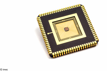
| At ISSCC, imec researcher Pamula Venkata Rajesh showed a readout chip for photoplethysmogram measurements (PPG) based on LED-light and using compressive sampling. The PPG results deduce both heart beat and heart rate variability. They are a nice alternative for ECG monitoring because they don’t require the use of electrodes on the patient’s chest. The downside is the sensor’s LED light that shines through the skin needing additional energy, which is a serious drain on the energy budget of the small sensor chip. Therefore, it is important that the measurements can be done with compressive sampling, measuring less but smarter data points. | |
 |
|
| Readout chip for photoplethysmogram measurements using compressive sampling. | |
| The future | |
| Thanks to these and other developments, sensors improve every day, ready to take their place in our environments and lives. Other technologies that will be needed in this IoT-scenario are collecting and interpreting big data in the cloud, flexible electronics, and new standards for low-power radios. Looking at the 16 ISSCC-contributions, we are well on our way to bringing the Internet of Things to reality. | |
|
By Nick Van Helleputte. Nick received his MS degree in electrical engineering in 2004 from the Katholieke Universiteit Leuven, Belgium. He received his Ph.D. degree from the same institute in 2009 (MICAS research group). His PhD research focused on low-power ultra-wide-band analog front-end receivers for ranging applications. He joined imec in 2009 as an Analog R&D Design Engineer. He initially worked in the space and extreme electronics group working on among others ESA projects and design of radiation hard, space-grade ASICs. He later moved to the biomedical circuits and systems design team which he is currently leading. His research focus is on ultra-low-power circuits for biomedical applications. He has been involved in analog and mixed-signal ASIC design for wearable and implantable applications. Nick is an IEEE member and served on the technical program committee of VLSI circuits symposium.
|
|
|
Become a Spotlight guest author! Join our large and growing group of guest contributors. Have you just published a scientific paper or have other exciting developments to share with the nanotechnology community? Here is how to publish on nanowerk.com. |
|