| Dec 15, 2025 |
Nanoscale metal structures let thermal photodetectors approach semiconductor speedsA metasurface-enhanced thermal photodetector achieves 125 picosecond response times, approaching semiconductor speeds without external power or cooling while retaining broad wavelength flexibility. |
| (Nanowerk Spotlight) Thermal photodetectors occupy a unique niche in sensing technology. Unlike semiconductor photodiodes that convert light directly into electrical signals through quantum effects, thermal detectors work through a two-step process: they first absorb light and convert it to heat, then transduce that temperature change into a measurable electrical response. |
| This fundamental mechanism gives thermal detectors a powerful advantage, as they can theoretically detect any wavelength of light, from visible to far infrared, simply by engineering the absorber layer. But this flexibility has always come at a steep cost: speed. |
| The problem is thermodynamics itself. Traditional thermal detectors rely on thick, blackened absorbing layers that soak up light across a broad spectrum. While effective at capturing photons, these bulky absorbers carry substantial thermal mass, meaning they heat up and cool down slowly as thermal energy diffuses through the material. |
| The result is response times measured in milliseconds, adequate for thermal imaging cameras or laser power meters, but impossibly slow for high-speed optical communications or ultrafast spectroscopy. |
| Pyroelectric detectors represent one major category of thermal photodetector. They exploit materials whose spontaneous electrical polarization changes with temperature. When light heats a pyroelectric material, its internal electric dipoles shift, generating a current proportional to the rate of temperature change. |
| Materials like lithium tantalate and triglycine sulfate have served as pyroelectric sensing elements, but even the best conventional designs struggle to break the millisecond barrier. |
| Meanwhile, nanophotonics has made remarkable strides in controlling light at the nanoscale. Metallic nanostructures can act as optical antennas, concentrating electromagnetic energy into volumes far smaller than the wavelength of light. |
| When engineers arrange these structures into carefully designed metasurfaces, they can absorb specific wavelengths with near-perfect efficiency while reflecting others. The absorbed energy dissipates as heat on picosecond timescales, raising a compelling question: what if the sluggish blackened absorbers of traditional thermal detectors could be replaced with these ultrafast, spectrally selective nanophotonic structures? |
| A research team at Duke University, collaborating with the Air Force Research Laboratory and KBR, has now demonstrated that this approach can push pyroelectric photodetectors into the gigahertz regime. Their study, published in Advanced Functional Materials ("Metasurface‐Enhanced Thermal Photodetector Operating at Gigahertz Frequencies"), reports devices achieving 3 dB bandwidths of 2.8 GHz, corresponding to a rise time of just 125 ps. This represents the fastest pyroelectric photodetector reported to date, challenging the assumption that thermal detectors must inherently be slow. |
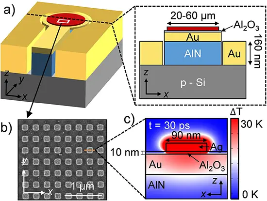 |
| a) Schematic representation of metasurface-enabled photodetectors illustrating key dimensions with b) SEM image of the metasurface absorber. The red area represents the metasurface array. c) Finite element simulations of a single plasmonic nanostructure showing a cross-section of the pyroelectric layer 30 ps after resonant excitation of the metasurface. (Image: Reproduced with permission from Wiley-VCH Verlag) |
| The detector architecture couples a metallic metasurface with a thin pyroelectric film of aluminum nitride. The metasurface consists of nanoscale silver square prisms, measuring 90 nm × 90 nm × 35 nm, arranged in an array atop a gold film. A 10 nm layer of aluminum oxide separates the nanostructures from the gold, creating what physicists call a nanogap cavity. |
| This geometry acts as a precision optical antenna. When near-infrared light at the resonant wavelength of approximately 790 nm strikes the surface, the metallic nanostructures absorb over 95% of incident photons rather than reflecting them. Light at other wavelengths bounces away. |
| Resistive losses in the metals convert the absorbed optical energy to heat within picoseconds. This heat then conducts through the gold film into the underlying aluminum nitride layer, which measures roughly 160 nm thick. The aluminum nitride sits atop a heavily doped silicon wafer that serves as an electrical contact, forming a capacitor structure. When heat reaches the aluminum nitride, its spontaneous polarization changes, generating a transient current. |
| Finite element simulations reveal the thermal dynamics in striking detail. Light converts to heat within 5 ps, and this heat reaches the aluminum nitride layer within 30 ps. The temperature change rate, which drives pyroelectric current, peaks just 4 ps after heat generation begins in the nanostructures. These extraordinarily fast thermal processes indicate that photothermal conversion does not limit the fundamental response time. |
| The researchers fabricated devices with active areas ranging from 0.3 × 10⁻³ mm² to 2.9 × 10⁻³ mm², corresponding to diameters between 20 and 60 μm. For devices with a 1.3 × 10⁻³ mm² active area, peak responsivity reached 1.64 mA W⁻¹ at the resonant wavelength, nearly 100 times higher than control devices using a plain gold film. The noise equivalent power, which quantifies the minimum detectable optical signal, reached values as low as 96 pW Hz⁻¹/². |
| Smaller devices exhibited higher bandwidths. The smallest functional devices, with 0.3 × 10⁻³ mm² active areas, achieved bandwidths of 2.80 ± 0.08 GHz. Electrical characterization revealed that device capacitance scaled with area, ranging from 1.1 to 2.4 pF. The measured bandwidths matched predictions based on the RC time constant, a value determined by multiplying electrical resistance and capacitance that governs how quickly charge moves through a circuit. |
| This finding carries an important implication: even the smallest devices remain limited by their electrical characteristics rather than their thermal response. The thermal conversion happens faster than the electrical readout can follow. |
| Simulations suggest that overcoming electrical limitations through improved fabrication could yield response times as fast as 30 ps, comparable to carrier-limited response times in commercial semiconductor photodiodes. |
| The devices require no external power or bias voltage, functioning entirely through the pyroelectric effect at room temperature. Their active layers total only 285 nm in thickness, making them compatible with on-chip integration. The spectral selectivity from the metasurface opens possibilities for multispectral imaging or polarimetry by engineering different resonant wavelengths into detector arrays. |
| The path toward even faster devices now appears clear. Higher sensitivity would enable smaller active areas with lower capacitance. Alternative pyroelectric materials with larger pyroelectric coefficients, such as lithium niobate, zinc oxide, or zirconium-doped hafnium oxide, might boost responsivity further. |
| Optimizing pyroelectric layer thickness presents a trade-off: thicker films reduce capacitance but slow thermal transfer, while thinner films accelerate thermal response but increase capacitance. |
| These results demonstrate that thermal photodetectors need not sacrifice speed for wavelength flexibility. By replacing traditional blackened absorbers with engineered metasurfaces, this collaboration has shown that pyroelectric devices can operate at speeds approaching semiconductor photodiodes while detecting any wavelength where an appropriate absorber can be designed. |
 By
Michael
Berger
– Michael is author of four books by the Royal Society of Chemistry:
Nano-Society: Pushing the Boundaries of Technology (2009),
Nanotechnology: The Future is Tiny (2016),
Nanoengineering: The Skills and Tools Making Technology Invisible (2019), and
Waste not! How Nanotechnologies Can Increase Efficiencies Throughout Society (2025)
Copyright ©
Nanowerk LLC
By
Michael
Berger
– Michael is author of four books by the Royal Society of Chemistry:
Nano-Society: Pushing the Boundaries of Technology (2009),
Nanotechnology: The Future is Tiny (2016),
Nanoengineering: The Skills and Tools Making Technology Invisible (2019), and
Waste not! How Nanotechnologies Can Increase Efficiencies Throughout Society (2025)
Copyright ©
Nanowerk LLC
|
|
|
|
ORCID information
|

Become a Spotlight guest author! Join our large and growing group of guest contributors. Have you just published a scientific paper or have other exciting developments to share with the nanotechnology community? Here is how to publish on nanowerk.com. |
