| Posted: Sep 08, 2006 |
Colloidal crystals of ordered microspheres - a new class of advanced materials |
| (Nanowerk Spotlight) Colloidal crystals constructed by monodispersed microspheres packed in ordered arrays represent a new class of advanced materials that are useful in many areas. For example, due to their novel light diffraction and photonic bandgap properties, colloidal crystals are promising elements in the fabrication of devices such as optical filters and switches, chemical and biochemical sensors, and photonic chips. Various self-assembly techniques have been developed to form colloidal crystals on different substrates, including the flow-cell methods, vertical deposition, micromolding in capillaries and so on. Although existing methods can provide colloidal crystals of different structures and quality, efficient approaches to high stability and large scale colloidal crystals are increasingly attracting attention. Generating ordered microstructures in the colloidal crystal films and colloidal crystals with different structures and configurations are particularly important in the fabrication of optical devices. |
| Professor Bai Yang, director of the The Key Laboratory for Supramolecular Structure and Materials of Ministry of Education at Jilin University/PR China, and his group have developed a number of methods to organize polymeric, inorganic, even composite microspheres into various structures, generating various properties and functions. |
| "Using these methods" Yang explains to Nanowerk, "we prepared various colloidal crystals with different structures. These included colloidal crystals with ordered voids and two- or three-dimensional (2D or 3D) patterned arrays, colloidal crystals on non-planar surfaces, heterogeneous colloidal crystals of different building blocks, colloidal crystals composed of non-spherical polyhedrons, and particularly colloidal crystals of non-close-packed (ncp) colloidal microspheres." |
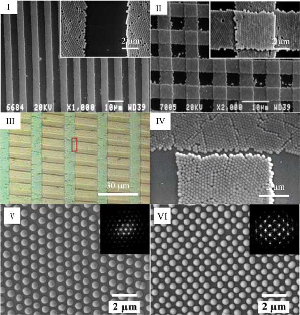 |
| (I, II) SEM images of 2D and 3D patterned colloidal crystals fabricated by lift-up process. (III) Optical photograph of the patterned heterogeneous colloidal crystal using a two-step µCP procedure. (IV) High magnification SEM image of a crossover of two crystal film lines in figure (III). (V) SEM image of the hexagonal ncp array on a PVA-coated substrate fabricated by swelling the PDMS film with pure toluene. (VI) SEM images of 2D ncp arrays with square lattice fabricated by stretching the PDMS. (Source: Dr. Bai Yang) |
| Yang explains that by applying lift-up soft lithography and micro-contact printing (µCP) to colloidal crystals, they have developed versatile approaches to patterned colloidal crystals of various structures. |
| "Using these approaches we can transfer colloidal crystals intentionally, achieving patterned colloidal crystals on both the planar and nonplanar substrates, as well as heterogeneous colloidal crystal films" he says. |
| Based on the solvent-swelling and mechanical deformation behaviors of PDMS elastomers, the researchers have developed a simple technique to fabricate ncp microsphere arrays with designable lattice structures, which are difficult to obtain by conventional self-assembly methods. This technique provides a simple and flexible route for creating microlens arrays and adjustable templates for the systematic study of the epitaxial growth of 3D colloidal crystals, and for the fabrication of novel nanostructures, such as ordered arrays of nanoholes or nanodots on various substrates. |
| "Using various colloidal crystals obtained as templates, we established several methods to generate surface patterns with different structures ranging from nanoscale to micron-scale. Particularly, we have intentionally applied 3D self-assembled colloidal crystals in preparing 2D nanostructures on different substrates." |
| "In brief, our methods should hold considerable promise in nanofabrication, nanosensing, microreactors, and control of colloidal crystallization" Yang concludes. |
| The findings were published in a paper titled "Fabricating colloidal crystals and construction of ordered nanostructures" in the July 28, 2006 online edition of the new, free-access publication Nanoscale Research Letters. |
 By
Michael
Berger
– Michael is author of four books by the Royal Society of Chemistry:
Nano-Society: Pushing the Boundaries of Technology (2009),
Nanotechnology: The Future is Tiny (2016),
Nanoengineering: The Skills and Tools Making Technology Invisible (2019), and
Waste not! How Nanotechnologies Can Increase Efficiencies Throughout Society (2025)
Copyright ©
Nanowerk LLC
By
Michael
Berger
– Michael is author of four books by the Royal Society of Chemistry:
Nano-Society: Pushing the Boundaries of Technology (2009),
Nanotechnology: The Future is Tiny (2016),
Nanoengineering: The Skills and Tools Making Technology Invisible (2019), and
Waste not! How Nanotechnologies Can Increase Efficiencies Throughout Society (2025)
Copyright ©
Nanowerk LLC
|

Become a Spotlight guest author! Join our large and growing group of guest contributors. Have you just published a scientific paper or have other exciting developments to share with the nanotechnology community? Here is how to publish on nanowerk.com.
