| Posted: Dec 14, 2017 |
Taking ice lithography to the next level |
| (Nanowerk Spotlight) Lithography is a key technology for the production of semiconductor devices. It is used to define nanoscale patterns on computer chips. Electron beam lithography (EBL) is a type of lithography that is applied to both small scale production and academic research. |
| Recent developments in multi-electron beam lithography technology has increased the EBL through-put about 100000 times. In academic research, EBL has been the back-bone technology for making nanophotonic, nanoelectronic, graphene, nanopore DNA sequencing, and quantum devices. |
| Established lithography protocols require samples that are mirror polished with high optical smoothness, which essentially limits processing to two dimensions. This is one of the reasons why active components on semiconductor and nanodevices are on the surface of the semiconductor, while the bulk material is unused. A very important part of the lithography process is the spinning, baking and development of resist which require dedicated instruments and cleanroom laboratory facility. |
| "We discovered that ices of simple organic molecules such as alcohols (isopropanol), and nonane (main component of diesel) can be nanopatterned by a focused electron beam (e-beam)," Anpan Han, an assistant professor at the National Center for Micro- and Nanofabrication at Technical University of Denmark (DTU Danchip), tells Nanowerk. "All the organic ices we have tried so far reacted to e-beam exposure by forming a solid non-volatile product, and hence they can be used as EBL resist. Our results showcase many advantages compared to the state-of-the-art in EBL." |
| As Han and his colleagues have reported in Nano Letters ("Organic Ice Resists"), their entire 3D lithography process takes place in a single vacuum instrument and avoids exposing users to chemicals and the need for cleanrooms. |
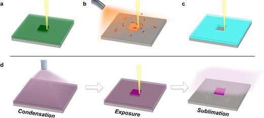 |
| OIR patterning compared to other e-beam based techniques. (a) EBL: The sample is coated with a resin layer that changes its solubility when exposed to the e-beam. The sample is then removed from the vacuum instrument and the pattern is developed with dedicated solvents. (b) FEBID: A precursor is introduced in the vacuum chamber through a nozzle, it is adsorbed onto the surface and dissociates due to the electron bombardment during exposure, depositing a nonvolatile product. (c) IL: Water vapor is condensed onto a cryogenically cooled sample to form an ice thin-film, which is removed by the e-beam. The patterned ice is used as mask for in situ processes before bringing the sample back to room temperature. (d) OIR: A vapor of a simple organic compound is first condensed onto the cooled sample to form a uniform layer. Its interaction with the e-beam locally modifies its chemical composition, resulting in a nonvolatile product. When the sample is heated to room temperature, the unexposed OIR sublimates while the exposed patterns are stable, enabling ambient downstream processing. (Reprinted with permission by American Chemical Society) |
| With organic ice resist (OIR) technology, nanolithography can be made accessible to more scientists. |
| The DTU scientists were inspired and motivated by ice lithography (see: "Nanotechnology on ice – novel lithography approach to nanodevice fabrication") and focused electron beam induced deposition (FEBID), which are both 3D lithography technologies. |
| In OIR, first the researchers patterned down to 10 nm onto very fragile samples using one instrument without any spin, bake and development steps (which require an expensive cleanroom environment). Then they created 3D layered structures in situ using iterative condensation-exposure-sublimation steps. |
| For thick layers, they can process 3 orders of magnitude faster than in focused electron induced deposition (FEBID), which is the 3D e-beam patterning method of choice. |
| They also demonstrated that organic ice resists can be used for making diamond nanopillars for quantum sensing applications. The organic ice material they use is also very sustainable and inexpensive compared to EBL resists. |
| The scientific core of these findings is that the physical and chemical processes occurring when a lithography resist is exposed to a source of irradiation at room temperature are also happening to organic molecules frozen at cryogenic temperature. |
| "In general, low temperature physics can be very different than room temperature physics, since processes like diffusion of atomic species or ions or radicals are evolving in a 'cold' environment where everything is slow," explains Marco Beleggia, Associate Professor at DTU Danchip. "Yet, OIR technology works, performs similarly to room-temperature EBL, and provides us with a new, flexible nanopatterning method where the only step required after exposure is warming up to let the unexposed resist evaporate." |
| "Since we have not yet been able to identify the chain of chemical steps leading from the unexposed frozen layer of organic molecules to the stable end-product, we are now focusing our efforts on studying the interactions between beam electrons and the target molecules to fully understand the science behind OIR technology," he adds. |
| This animation illustrates organic ice resist processing, which shares features with 3D printing. (Video: DTU) |
| The short-term implication of this work is to provide researchers with a new nanoscale 3D printing technology. OIR also shows great potential to enable next-generation quantum sensors. |
| The long-term implications might have a revolutionary impact on semiconductor production and computing. "As the technology matures, and processing speed approaches EBL, we believe that by combining OIR with multi-electron-beam and other 3D technologies, semiconductors can be packed in the third dimension," says Han. "This would allow us to use the whole bulk semiconductor material, which today is serving as the supporting substrate for the device layer that is only a few tens of nanometers. Being able to use the several millimeter thick semiconductor substrate would increase the density of processing units by many orders of magnitude." |
| Going forward, the DTU researchers are focusing their efforts on achieving three goals: |
| 1) Understand the fundamental science of electron-organic ice interactions |
| To that end they are performing in situ experiments in the transmission electron microscope (TEM) and characterizing final exposure products with advance spectroscopy techniques. Understanding ice formation under electron irradiation will not only improve the lithography process, but also answer more fundamental questions about electron beam-matter interactions. |
| "Once we acquire this knowledge we can use it to select the optimal 3D lithography organic molecule from the vast databases of organic chemistry, and streamline the process to increase its efficiency and speed even more," Han points out. |
| 2) To investigate the ultimate resolution of the OIR technology |
| Both nonane and anisole ices are formed by very small molecules: a linear nine carbons chain and an aromatic ring, respectively. This means that they have the potential to produce very small structures with improved line-edge roughness. |
| "Currently, the resolution in our SEM-based system is limited by the instrument itself," says William Tiddi, the PhD student who has built it as a first step of his project. "To overcome these limitations, we patterned OIR in an environmental transmission electron microscope (ETEM). We used the built-in gas cell and cryo holder to introduce nonane gas to the microscope and condense a sub-10 nm thick ice layer on a 5-nm-thin Si3N4 TEM membrane. In the Nano Letters paper we achieved 10 nm dot arrays, but we want to know how far we can push forward." |
| 3) Applications for quantum sensing technology |
| Leading scientists in quantum sensing predict a significant increase in sensitivity if 3D structures could be added to the current 2D sensors. By improving their custom instrument and process, the team hopes to contribute to the quantum sensing effort. |
| According to the team, the major challenge for this research is the availability of adequate instrumentation. There are three systems in the world that can process OIR, and they are located at Harvard University, Zhejiang University and DTU. |
| "While we are actively pursuing technology transfer to an industry partner to make our technology commercially available, we will be more than happy to provide instrumentation assistance to interested researchers and scientists," Han notes. |
| "There are many research directions beyond lithography," the team concludes. "Organic chemistry is one of the five branches of chemistry, and we think many organic chemists might be very interested in OIR technology. Also, our work could potentially stimulate research in hybrid organic-inorganic systems at the boundary between life and material sciences." |
 By
Michael
Berger
– Michael is author of four books by the Royal Society of Chemistry:
Nano-Society: Pushing the Boundaries of Technology (2009),
Nanotechnology: The Future is Tiny (2016),
Nanoengineering: The Skills and Tools Making Technology Invisible (2019), and
Waste not! How Nanotechnologies Can Increase Efficiencies Throughout Society (2025)
Copyright ©
Nanowerk LLC
By
Michael
Berger
– Michael is author of four books by the Royal Society of Chemistry:
Nano-Society: Pushing the Boundaries of Technology (2009),
Nanotechnology: The Future is Tiny (2016),
Nanoengineering: The Skills and Tools Making Technology Invisible (2019), and
Waste not! How Nanotechnologies Can Increase Efficiencies Throughout Society (2025)
Copyright ©
Nanowerk LLC
|

Become a Spotlight guest author! Join our large and growing group of guest contributors. Have you just published a scientific paper or have other exciting developments to share with the nanotechnology community? Here is how to publish on nanowerk.com. |
