| Mar 22, 2022 |
Kirigami-style, self-folding circuit boards |
| (Nanowerk Spotlight) In an effort to develop simpler ways to fabricate complex 3D (nano)structures for use in electronics and other areas, researchers have repeatedly made use of kirigami at the nanoscale (see for instance our previous Nanowerk Spotlight on "kirigami-structured graphene-polymer hybrid nanocomposite for strain sensors"). |
| Kirigami enhances the Japanese art form of origami, which involves folding paper to create 3D designs, by strategically incorporating cuts to the paper prior to folding. The method enables artists to create sophisticated three-dimensional structures more easily. |
| Many origami-style self-folding systems rely on stimuli-responsive polymers that fold in response to heat, light, etc. For instance, the world's smallest origami bird was created by micron-sized shape memory actuators that enable nanometer-thin layers to fold themselves into 3D configurations. All it requires is a quick jolt of voltage. |
| In a problem for manufacturing 3D-shaped electronic components, rather than the traditional planar structures, most self-folding processes use materials that are either poor electrical conductors or incompatible with conventional electronic processing. |
| Addressing this issue, researchers have now demonstrated rapid cutting and folding of a printed circuit board (PCB) into complex 3D electronics using only a simple laser cutter. |
| The results have been published in ACS Applied Materials & Interfaces ("Self-Folding PCB Kirigami: Rapid Prototyping of 3D Electronics via Laser Cutting and Forming"). |
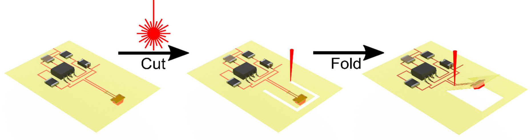 |
| Figure 1. Schematic of the process of cutting and laser forming (folding) a flexible PCB into a 3D shape using the same laser. Surface mount components are soldered to the board before the laser cuts out the fold region before laser forming to produce the 3D structure. (Reprinted with permission by American Chemical Society) |
| This origami manufacturing technology has the potential to allow faster and cheaper production of 3D electronic devices based on thin shells such as antennas that are poorly suited for current 3D printing methods. |
| "Our technique relies on a method known as laser forming, where heat from a focused laser generates bending within a target," Michael D. Dickey, the Camille and Henry Dreyfus Professor in the Dept. of Chemical & Biomolecular Engineering at North Carolina State University, explains to Nanowerk. "Being able to rapidly fold electronics using only a widely available machine tool without any manual handling is a major innovation in 3D electronics fabrication." |
| Laser forming is well known for bending large metal sheets in fields like construction and ship building. This process is realized by introducing thermal stresses into the surface of a workpiece, thereby inducing plastic strains that bend the material. |
| However, as the researchers point out, origami-based folding of a printed circuit board with copper tens of micrometers thick, as in this work, required substantial improvements in the control of the technique, most notably through controlling the light absorption through using laser heating to grow oxides on the surface (see this previous paper in Advanced Materials Technologies: Laser Forming for Complex 3D Folding). |
| The team used a pulsed fiber laser to both cut and fold flexible PCBs that have been patterned and populated with surface mount components as depicted in Figure 1 above. |
| "We used this technique to produce complex 3D structures with electronically functional circuits," says Dickey. "At higher powers, the laser ablates the copper and the polyimide in the substrate, but at carefully controlled lower powers the substrate is simply heated, allowing the same laser system to be used for both cutting and laser forming of the flex-PCBs." |
| The team also points out that origami manufacturing is ideally positioned to address a major limitation of many 3D printers: that the thin conductors and shapes for devices like antennas are very difficult to print without long print times and sacrificial supports. |
| In addition, this is also a fully hands-free method for cutting and folding complex electronics and other structures. |
| This video shows laser forming of a circuit board cube with integrated LED. |
| "We see this technique as both being ideal for the casual hobbyist or maker with access to a laser cutter, giving them the opportunity to build functional 3D electronics, as well as being well positioned for more traditional origami applications such as unfolding space-based systems from compact packages for transport," Dickey notes. |
| He referred to a recent example, where the James Webb Space Telescope required tens of individual motors to unfold structures like their sunshield, and the entire scientific community was terrified by the possibility of a single motor failing and dooming the telescope. Being able to unfold large arrays of solar cells using only a simple light source would be revolutionary. |
| The team is currently using their technology to fabricate both sensors and antennas, two applications that benefit strongly from 3D structuring, and where origami manufacturing could turn out to be an ideal approach to these types of applications. |
| "I think there is a great potential for looking at both new materials and applications for origami manufacturing," Dickey concludes. "One particular challenge that we're interesting in looking at is improved computational design tools to make origami more accessible to the casual user like the tools available to the 3D printing community." |
 By
Michael
Berger
– Michael is author of four books by the Royal Society of Chemistry:
Nano-Society: Pushing the Boundaries of Technology (2009),
Nanotechnology: The Future is Tiny (2016),
Nanoengineering: The Skills and Tools Making Technology Invisible (2019), and
Waste not! How Nanotechnologies Can Increase Efficiencies Throughout Society (2025)
Copyright ©
Nanowerk LLC
By
Michael
Berger
– Michael is author of four books by the Royal Society of Chemistry:
Nano-Society: Pushing the Boundaries of Technology (2009),
Nanotechnology: The Future is Tiny (2016),
Nanoengineering: The Skills and Tools Making Technology Invisible (2019), and
Waste not! How Nanotechnologies Can Increase Efficiencies Throughout Society (2025)
Copyright ©
Nanowerk LLC
|

Become a Spotlight guest author! Join our large and growing group of guest contributors. Have you just published a scientific paper or have other exciting developments to share with the nanotechnology community? Here is how to publish on nanowerk.com. |
