| Posted: May 31, 2016 | |
Nanotechnology's tiny steps toward atomic-scale 3D fabrication |
|
| (Nanowerk Spotlight) Over the past few decades, the development of electron microscopy has gone hand in hand with techniques for atomically precise fabrication of 3D structures based on electron and ion beams. | |
| All material functionality is governed by the type, arrangement, and bonding of atoms. Enabling the capacity to perform atomically precise directed assembly of matter will open the doors to emerging technologies in computing, energy, catalysis, and a plethora of other fields. | |
| A recent review article in ACS Nano ("Directing Matter: Toward Atomic-Scale 3D Nanofabrication") illustrates the use of focused electron and ion beams (e-beams and i-beams) to induce highly localized chemical reactions at solid-vapor and solid-liquid interfaces, amorphous to crystalline phase transformations with atomic layer precision, and the motion of specific single dopant atoms within crystal lattices, thus laying the foundation for atomically precise directed assembly of materials and devices. | |
| The growth of plasmonic gold nanostructures by electron beam induced deposition (EBID) has been demonstrated already 10 years ago and the physics behind this nanofabrication technique has been explored (see for instance: "Scientists unveil new physics behind the nanofabrication technique of electron beam induced deposition"). The process has been improved over the years and researchers are now able to grow structures much faster with a broad range of precursors (see: "A new process for rapidly fabricating complex 3D nanostructures"). | |
| In their review, the authors emphasize the synergy between imaging, nanofabrication, and modeling in order to reveal the fundamental mechanisms of charged particle-surface interaction. | |
| They present several recent examples that suggest the feasibility of atomically precise fabrication in the bulk, including creating specific dopant configurations, ordered vacancy planes, and other structures. | |
| The article covers EBID/IBID from gas or liquid precursors, e-beam-induced crystallization in the bulk, and the ability to image and to analyze single atoms and defects in 2D structures. | |
 |
|
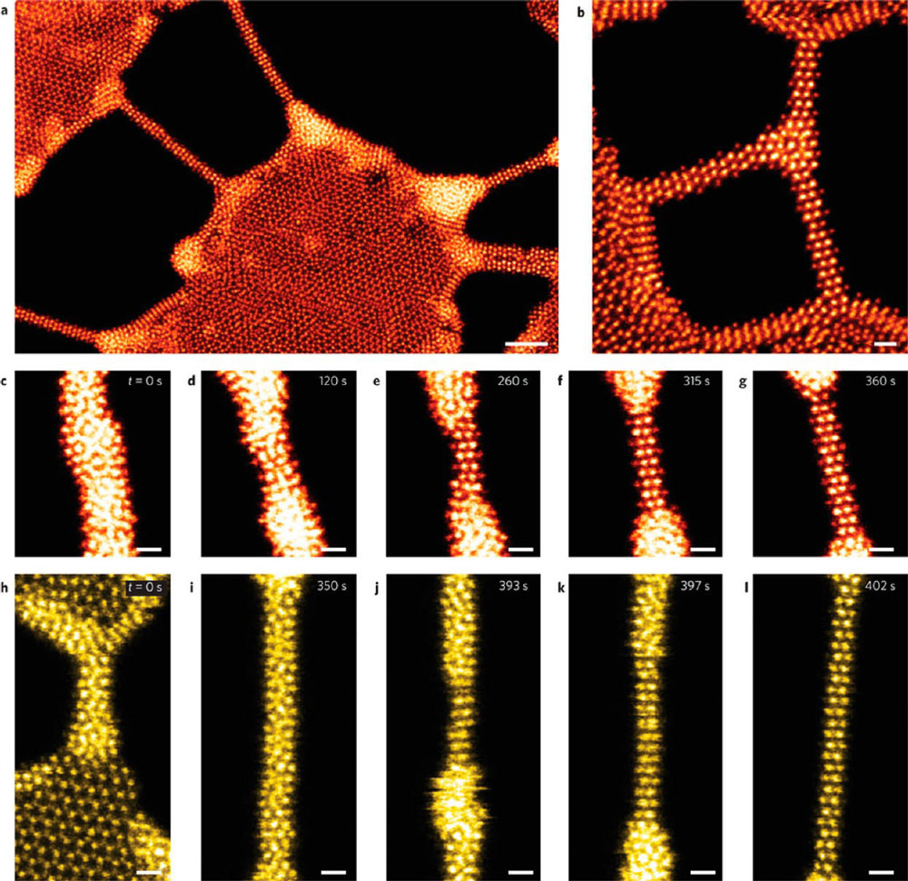
| (a) Patterning of a MoSe nanowire network, where each nanowire is sculpted individually. (b) Ramified Y junction made of three MoSe nanowires. (c-l) Serial snapshots of the sculpting process of individual MoSe (c-g) and MoS (h-l) nanowires. All images are STEM Z-contrast images, false-colored for better visibility. Scale bars, 2 nm (a), 0.5 nm (b-l). (© Nature Publishing Group) (click on image to enlarge) | |
| Electron-beam/ion-beam-induced deposition from gas precursors | |
| Discussing Focused Electron-Beam-Induced Processing – a nanoscale direct-write synthesis technique where an electron beam directs assembly of a surface-adsorbed precursor via an electron-stimulated chemical reaction – and Focused Ion-Beam-Induced Processing – where the deposition and etching of nanoscale materials is induced by a focused ion beam – the authors show how these techniques were developed; they discuss their benefits but also obstacles to large-scale implementation. | |
| Eelectron-beam/ion-beam-induced deposition from liquid precursors | |
| An alternative pathway to using gas precursors for direct nanofabrication is direct-write with electron and/or ion beams with a liquid precursor. This method utilizes the e-beam or i-beam as an ionizing source that decomposes solvent molecules to generate solvated electrons and other radicals in a complex cascade of reaction pathways. | |
| When using electrons to direct-write in solution, the minimal size of the created structures is limited to the nanometer scale due to the fundamental physics of the interactions between the electron beam and the liquid, including the lateral transport of solvated electrons and ionic species. The helium ion beam, on the other hand, might offer the potential for improved resolution. | |
| Atomically precise e-beam-induced crystallization in the bulk | |
| E-beam and i-beam patterning are popular and versatile approaches for creating structures on ∼10-100 nm scales, typically in SEM-like geometry. However, in the field of imaging, high-resolution transmission electron microscopy (TEM) has long been a tool of choice because it allows for atomic-scale studies of crystals and nanoparticles. | |
| As the authors note, over the last 15 years, aberration correction has pushed the achievable resolution into the sub-angstrom range and allowed for much greater localization of the probe in STEM geometry, suggesting that higher precision patterning should be achievable using these improved electron probes. | |
| Provided that the electron beam path can be programmed, localization of features in the areas illuminated by the beam and the ability to control their growth allows for more complex patterning. | |
| The team writes that the manufacturing of epitaxial crystalline nanostructures with predefined shapes is particularly interesting, as adjustable strain states could yield ways to control properties, and the ordered final structures can be more easily modeled than amorphous structures. | |
 |
|
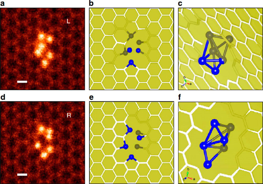
| (a,d) ADF Z-contrast images of two representative stable Si6 cluster configurations embedded in a graphene pore. (b,e) Two- and (c,f) three-dimensional structures obtained from first-principles calculations. Si and C atoms below the graphene plane are shaded. L or R labels are used to highlight when the oscillating Si atom is either at the left or right sites. Scale bar, 0.2 nm. (© Nature Publishing Group) (click on image to enlarge) | |
| Single-atom dynamics and beyond | |
| The difficulties in manipulating single atoms for nanoscale engineering were famously highlighted by Stemmer ("Three-dimensional imaging of individual dopant atoms in SrTiO3"). | |
| The use of an electron beam might provide an answer to this dilemma by allowing the direct addressing of single atoms in bulk 3D materials. | |
| The review highlights results ("Direct Observation of Dopant Atom Diffusion in a Bulk Semiconductor Crystal Enhanced by a Large Size Mismatch") that show the interplay between the materials science aspect of calculated diffusion barriers and the energy supplied to the sample by the electron beam. | |
| As the authors point out: "This relation is important because it is possible to directly control the accelerating voltage in a (S)TEM, thereby altering the energy transferred to the material. This concept raises several tantalizing prospects for the future as to what extent the final position of the dopant can be controlled. If single dopants could be directly manipulated, an obvious application would be toward quantum computing." | |
| Link theory and data | |
| Increasing computer power and more sophisticated analytical software allows analyzing experimental data in near real-time. This provides the ability to have rapid feedback to and from models and simulations that both inform and validate the simulations/model, which may ultimately provide predictive capabilities to guide experiments. | |
| Until recently, advances in microscopy relied on improvements in the instrumentation platforms, focused probes, lenses, detectors, measurement modalities, and mathematical tools for extraction of materials-specific parameters from imaging data. However, in almost all cases, due to the complexity and size of the available signals, only a small, manually selected subset of the fully generated information volume is recorded and an even smaller subset of this is processed. | |
| In the future, new tools will allow the (real-time) monitoring and analysis of the full data stream from the microscope. This would also allow researchers to take full advantage of all of the information contained in experimental data to provide input into computational methods to predict and understand materials. | |
| The authors conclude that "in order to see what is happening as it is happening, a significant emphasis must be placed on forming a tight loop between expansive dynamic streaming EELS (electron energy loss spectroscopy), tomographic, and ptychographic data sets provided by experimental platforms and the model-driven interpretation of the data. As the techniques mature, these theory-in-the-loop approaches will also significantly expedite the quality control process, an important facet in transitioning from scientific test-beds to high-volume manufacturing." | |
 By
Michael
Berger
– Michael is author of three books by the Royal Society of Chemistry:
Nano-Society: Pushing the Boundaries of Technology,
Nanotechnology: The Future is Tiny, and
Nanoengineering: The Skills and Tools Making Technology Invisible
Copyright ©
Nanowerk LLC
By
Michael
Berger
– Michael is author of three books by the Royal Society of Chemistry:
Nano-Society: Pushing the Boundaries of Technology,
Nanotechnology: The Future is Tiny, and
Nanoengineering: The Skills and Tools Making Technology Invisible
Copyright ©
Nanowerk LLC
|
|
|
Become a Spotlight guest author! Join our large and growing group of guest contributors. Have you just published a scientific paper or have other exciting developments to share with the nanotechnology community? Here is how to publish on nanowerk.com. |
|